54AC280DMQB National Semiconductor, 54AC280DMQB Datasheet
54AC280DMQB
Specifications of 54AC280DMQB


Related parts for 54AC280DMQB


54AC280DMQB Summary of contents
Page 1
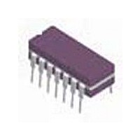
... Data Inputs 0 8 Odd Parity Output O Even Parity Output E FACT ™ trademark of Fairchild Semiconductor Corporation. © 1998 National Semiconductor Corporation DS100359 September 1998 Features n I reduced by 50 9-bit width for memory applications n Standard Microcircuit Drawing (SMD) 5962-92201 Connection Diagrams Pin Assignment for ...
Page 2
Logic Diagram Please note that this diagram is provided only for the understanding of logic operations and should not be used to estimate propagation delays. www.national.com 2 DS100359-5 ...
Page 3
... Absolute Maximum Ratings If Military/Aerospace specified devices are required, please contact the National Semiconductor Sales Office/ Distributors for availability and specifications. Supply Voltage ( Input Diode Current ( −0. 0. Input Voltage (V ) −0. Output Diode Current ( −0. 0. Output Voltage (V ) −0. Output Source or Sink Current ( Ground Current ...
Page 4
DC Characteristics for ’AC Family Devices Symbol Parameter I Maximum Quiescent CC Supply Current Note 2: All outputs loaded; thresholds on input associated with output under test. Note 3: Maximum test duration 2.0 ms, one output loaded at a time. ...
Page 5
Physical Dimensions inches (millimeters) unless otherwise noted 20 Terminal Ceramic Leadless Chip Carrier 14 Lead Ceramic Dual-In-Line Package NS Package Number E20A NS Package Number J14A 5 www.national.com ...
Page 6
... National Semiconductor Asia Pacific Customer Fax: +49 (0) 1 80-530 85 86 Response Group Email: europe.support@nsc.com Tel: 65-2544466 Fax: 65-2504466 Tel: +49 (0) 1 80-532 78 32 Email: sea.support@nsc.com Tel: +49 (0) 1 80-534 16 80 National Semiconductor Japan Ltd. Tel: 81-3-5620-6175 Fax: 81-3-5620-6179 ...