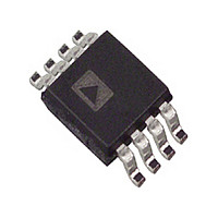
AD8315ARM-REEL Analog Devices Inc, AD8315ARM-REEL Datasheet - Page 15

AD8315ARM-REEL
Manufacturer Part Number
AD8315ARM-REEL
Description
Manufacturer
Analog Devices Inc
Datasheet
1.AD8315ARM-REEL.pdf
(24 pages)
Specifications of AD8315ARM-REEL
Operating Supply Voltage (typ)
3.3/5V
Operating Supply Voltage (min)
2.7V
Operating Supply Voltage (max)
5.5V
Operating Temp Range
-30C to 85C
Operating Temperature Classification
Commercial
Mounting
Surface Mount
Pin Count
8
Lead Free Status / RoHS Status
Not Compliant
Available stocks
Company
Part Number
Manufacturer
Quantity
Price
Company:
Part Number:
AD8315ARM-REEL
Manufacturer:
TOSHIBA
Quantity:
3 000
Part Number:
AD8315ARM-REEL
Manufacturer:
ADI/亚德诺
Quantity:
20 000
Company:
Part Number:
AD8315ARM-REEL7
Manufacturer:
AD
Quantity:
10 977
Company:
Part Number:
AD8315ARM-REEL7
Manufacturer:
microsemi
Quantity:
11 000
Part Number:
AD8315ARM-REEL7
Manufacturer:
ADI/亚德诺
Quantity:
20 000
Example
Assume that the gain magnitude of the power amplifier runs
from a minimum value of ×0.316 (−10 dB) at V
(40 dB) at V
V
30 dB directional coupler) and recalling that the nominal value
of V
the range of values needed for V
+33 dBm to −17 dBm. This can be found by noting that, in the
steady state, the numerator of Equation 7 must be 0, that is:
where V
the power amplifier output. For 33 dBm, V
evaluates to
For a delivered power of −17 dBm, V
Check that the power range is 50 dB, which should correspond
to a voltage change in V
which agrees.
Now, the value of V
parameter, inside the loop. It depends on the characteristics of
the power amplifier, and the value of the carrier amplitude V
Using the control values previously derived, that is, G
and V
−7 dBm (so V
Equation 11
both of which results are consistent with the assumptions made
about the amplifier control function. Note that the second term
is independent of the delivered power and a fixed function of
the drive power.
GBC
SLP
V
V
V
V
= (1.44 × 1)/0.48 − log
= 3.0 − 0.5 = 2.5 V
V
= (0.24 × 1)/0.48 − log
= 0.5 − 0.5 = 0
= 1 V. Using a coupling factor of k = 0.0316 (that is, a
GBC
SET
SET
SET
APC
APC
is 480 mV and V
IN
(max) = (V
(min) = (V
= V
(max) = 0.48 log
(min) = 0.48 log
= 1 V, and assuming the applied power is fixed at
is expanded to kV
APC
SLP
CW
= 2.5 V. Applying Equation 9, G
log
= 100 mV rms), the following is true using
10
APC
SET
SET
(kV
V
Z
V
is of interest, although it is a dependent
SET
GBC
= 316 μV for the AD8315, first calculate
GBC
PA
10
10
/V
of 50 dB × 24 mV/dB = 1.2 V,
)/V
)/V
10
10
(1 mV/316 μV) = 0.24 V
(316 mV/316 μV) = 1.44 V
PA
(0.0316 × 0.316 × 0.1/316 μV)
(0.0316 × 0.316 × 0.1/316 μV)
Z
)
, the fractional voltage sample of
SLP
SLP
SET
− log
− log
to control an output range of
PA
10
10
= 31.6 mV rms
kG
kG
PA
O
O
V
V
= 10 V rms, which
CW
CW
O
APC
/V
/V
= 0.316 and
Z
= 0 to ×100
Z
O
= 0.316
(12)
(13)
(14)
(15)
(16)
Rev. C | Page 15 of 24
CW
.
Finally, using the loop time constant for these parameters and
an illustrative value of 2 nF for the filter capacitor C
PRACTICAL LOOP
At present time, power amplifiers, or VGAs preceding such
amplifiers, do not provide an exponential gain characteristic. It
follows that the loop dynamics (the effective time constant)
varies with the setpoint because the exponential function is
unique in providing constant dynamics. The procedure must
therefore be as follows. Beginning with the curve usually provided
for the power output vs. the APC voltage, draw a tangent at the
point on this curve where the slope is highest (see Figure 35).
Using this line, calculate the effective minimum value of the
variable V
constant. Note that the minimum in V
maximum rate of change in the output power vs. V
For example, suppose it is found that, for a given drive power,
the amplifier generates an output power of P
P
This should be used to calculate the filter capacitance. The
response time at high and low power levels (on the shoulders
of the curve shown in Figure 35) is slower. Note also that it is
sometimes useful to add a 0 in the closed-loop response by
placing a resistor in series with C
this, see the Transient Response section.
2
at V
T
= (1/0.48)3.07 μs × 2 (nF) = 12.8 μs
V
O
GBC
DIRECTIONAL COUPLER
APC
= (V
= 20 (V
= V
GBC
GBC
Figure 34. Idealized Control Loop for Analysis
and use it in Equation 17 to determine the time
2
V
. Then, it is readily shown that
/V
IN
= kV
OF OVERALL CONTROL-
2
SLP
LOOP (EXTERNAL CAP)
− V
RESPONSE-SHAPING
V
) T
RF
SET
1
)/(P
2
− P
AD8315
1
)
V
FLT
RF
. For more information on
GBC
C
RF PA
FLT
corresponds to the
V
APC
1
at V
RF DRIVE: UP
TO 2.5GHz
V
CW
APC
APC
FLT
AD8315
= V
.
1
and
(18)
(17)


