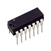
FAN4822IN_NL Fairchild Semiconductor, FAN4822IN_NL Datasheet - Page 7

FAN4822IN_NL
Manufacturer Part Number
FAN4822IN_NL
Description
Manufacturer
Fairchild Semiconductor
Datasheet
1.FAN4822IN_NL.pdf
(10 pages)
Specifications of FAN4822IN_NL
Start-up Supply Current
700uA
Switching Freq
87kHz
Operating Supply Voltage (min)
12.8V
Operating Supply Voltage (typ)
13.5V
Operating Supply Voltage (max)
14.2V
Operating Temp Range
-40C to 85C
Operating Temperature Classification
Industrial
Package Type
PDIP W
Pin Count
14
Mounting
Through Hole
Lead Free Status / RoHS Status
Compliant
PRODUCT SPECIFICATION
Q1 Turn-On
The turn-on event consists of the time it takes for the current
through L2 to ramp to the L1 current plus the resonant event
of L2 and the ZVS capacitor. The total event should occur in
a minimum of 350–450ns, but can be longer at the risk of
increasing the total harmonic distortion. Setting these times
equal should minimize conducted and radiated emissions.
Where I
The value of L2 is calculated to remain in discontinuous-
mode:
The resonant event occurs in 1/4 of a full sinusoidal cycle.
For example, when a 1/4 cycle occurs in 200ns, the fre-
quency is 1.25MHz.
Rearranging and solving for L2:
The resonant capacitor (C
equations 2 and 4 equal to each other and solving for C
Application
Figure 3 displays a typical application circuit for a 500W
ZVS PFC supply. Full design details are covered in applica-
tion note 33, FAN4822 Power Factor Correction With Zero
Voltage Resonant Switching.
REV. 1.0.1 8/10/01
L2
is equal to I
C
ZVS
f
RES
t
L2
Q1 OFF
=
=
=
---------------------------------------------------------------------------- -
V
---------------------------------------------------------------- -
2
---------------------------------- -
2
L2
L1
BUS
4 t
=
L2 C
.
V
=
t
ZVS
BUS
IL2
1
--------------------------
RES
4 t
V
2
) value is found by setting
2 P
+
RMS MIN
ZVS
t
2
RES
C
V
RES
ZVS
RMS MIN
OUT
=
2 P
2
=
---------------------
4 t
400ns
OUT
1
t
IL2
RES
t
IL2
ZVS
(3)
(4)
(5)
(2)
(1)
.
A. SYSTEM
CLOCK
(INTERNAL)
B. R
C. ZVS GATE (Q2)
D. VDS (Q2)
E. PFC GATE (Q1)
F. VDS (Q1)
G. I
L2
T
C
T
t
1
Figure 2. Timing Diagrams
t
2
t
3
FAN4822
7


