PCA9621D,118 NXP Semiconductors, PCA9621D,118 Datasheet - Page 5
PCA9621D,118
Manufacturer Part Number
PCA9621D,118
Description
IC BUS OUTPUT PORT 2WIRE 16SOIC
Manufacturer
NXP Semiconductors
Series
-r
Datasheet
1.PCA9621D118.pdf
(18 pages)
Specifications of PCA9621D,118
Supply Voltage (max)
5.5 V
Supply Voltage (min)
2.7 V
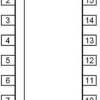
Package / Case
SO-16
Maximum Power Dissipation
300 mW
Mounting Style
SMD/SMT
Supply Current
1 uA
Lead Free Status / Rohs Status
Lead free / RoHS Compliant
Other names
568-6671-2


NXP Semiconductors
PCA9621
Product data sheet
7.6 A0, A1, A2 — address lines
7.7 Control register
The slave address of the PCA9621 is shown in
must be driven to a HIGH or LOW level—they are not internally pulled to a default state.
The read/write bit must be set LOW to enable a write to the Control register, or HIGH to
read from the Control register.
The Control register of the PCA9621 is shown in
can be activated independently by setting the appropriate bit in the Control register.
A LOW or ‘zero’ bit indicates that the respective channel (P7 to P0) is disabled
(high-impedance). The default reset condition of the register is all zeros, all ports
high-impedance. A HIGH or ‘one’ bit indicates the respective channel is active (sinking).
Example: Programming C1h (1100 0001b) into the Control register results in ports P0, P6
and P7 being ON (sinking) and the remaining ports being OFF (high-impedance).
Fig 4.
Fig 5.
Slave address
1 = ON (sinking)
0 = OFF (high-impedance)
Control register
All information provided in this document is subject to legal disclaimers.
Rev. 1 — 9 March 2011
MSB
1
P7
1
fixed
P6
0
P5
0
P4
A2
selectable
externally
P3
Figure
A1
Figure
P2
A0 R/W
65 mA 8-bit 2-wire bus output port
P1
4. The address pins (A2, A1, A0)
read = 1
write = 0
002aaf383
5. Each of the four output ports
P0
002aaf384
LSB
PCA9621
© NXP B.V. 2011. All rights reserved.
5 of 18
Related parts for PCA9621D,118
Image
Part Number
Description
Manufacturer
Datasheet
Request
R

Part Number:
Description:
65 mA 8-bit 2-wire bus output port
Manufacturer:
NXP [NXP Semiconductors]
Datasheet:

Part Number:
Description:
Pca9621 65 Ma 8-bit 2-wire Bus Output Port
Manufacturer:
NXP Semiconductors
Datasheet:
Part Number:
Description:
NXP Semiconductors designed the LPC2420/2460 microcontroller around a 16-bit/32-bitARM7TDMI-S CPU core with real-time debug interfaces that include both JTAG andembedded trace
Manufacturer:
NXP Semiconductors
Datasheet:

Part Number:
Description:
NXP Semiconductors designed the LPC2458 microcontroller around a 16-bit/32-bitARM7TDMI-S CPU core with real-time debug interfaces that include both JTAG andembedded trace
Manufacturer:
NXP Semiconductors
Datasheet:
Part Number:
Description:
NXP Semiconductors designed the LPC2468 microcontroller around a 16-bit/32-bitARM7TDMI-S CPU core with real-time debug interfaces that include both JTAG andembedded trace
Manufacturer:
NXP Semiconductors
Datasheet:
Part Number:
Description:
NXP Semiconductors designed the LPC2470 microcontroller, powered by theARM7TDMI-S core, to be a highly integrated microcontroller for a wide range ofapplications that require advanced communications and high quality graphic displays
Manufacturer:
NXP Semiconductors
Datasheet:
Part Number:
Description:
NXP Semiconductors designed the LPC2478 microcontroller, powered by theARM7TDMI-S core, to be a highly integrated microcontroller for a wide range ofapplications that require advanced communications and high quality graphic displays
Manufacturer:
NXP Semiconductors
Datasheet:
Part Number:
Description:
The Philips Semiconductors XA (eXtended Architecture) family of 16-bit single-chip microcontrollers is powerful enough to easily handle the requirements of high performance embedded applications, yet inexpensive enough to compete in the market for hi
Manufacturer:
NXP Semiconductors
Datasheet:
Part Number:
Description:
The XA-S3 device is a member of Philips Semiconductors? XA(eXtended Architecture) family of high performance 16-bitsingle-chip microcontrollers
Manufacturer:
NXP Semiconductors
Datasheet:

Part Number:
Description:
The NXP BlueStreak LH75401/LH75411 family consists of two low-cost 16/32-bit System-on-Chip (SoC) devices
Manufacturer:
NXP Semiconductors
Datasheet:
Part Number:
Description:
The NXP LPC3130/3131 combine an 180 MHz ARM926EJ-S CPU core, high-speed USB2
Manufacturer:
NXP Semiconductors
Datasheet:
Part Number:
Description:
The NXP LPC3141 combine a 270 MHz ARM926EJ-S CPU core, High-speed USB 2
Manufacturer:
NXP Semiconductors
Part Number:
Description:
The NXP LPC3143 combine a 270 MHz ARM926EJ-S CPU core, High-speed USB 2
Manufacturer:
NXP Semiconductors

Part Number:
Description:
The NXP LPC3152 combines an 180 MHz ARM926EJ-S CPU core, High-speed USB 2
Manufacturer:
NXP Semiconductors