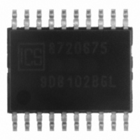
ICS9DB102BGLFT IDT, Integrated Device Technology Inc, ICS9DB102BGLFT Datasheet

ICS9DB102BGLFT
Specifications of ICS9DB102BGLFT
9DB102BGLFT
Available stocks
Related parts for ICS9DB102BGLFT
ICS9DB102BGLFT Summary of contents
Page 1
Two Output Differential Buffer for PCIe Gen1 & Gen2 Description The ICS9DB102 zero-delay buffer supports PCI Express clocking requirements. The ICS9DB102 is driven by a differential SRC output pair from an ICS CK410/CK505-compliant main clock. It attenuates jitter on the ...
Page 2
ICS9DB102 Two Output Differential Buffer for PCIe Gen1 & Gen2 Pin Configuration PLL_BW 1 CLK_INT 2 CLK_INC 3 **CLKREQ0# 4 VDD 5 GND 6 PCIEXT0 7 PCIEXC0 8 VDD 9 SMBDAT 10 Note: Pins preceeded by '**' have internal 120K ...
Page 3
ICS9DB102 Two Output Differential Buffer for PCIe Gen1 & Gen2 Absolute Max Symbol Parameter VDDA 3.3V Core Supply Voltage VDD 3.3V Output Supply Voltage Ts Storage Temperature Tcase Case Temperature Input ESD protection human body model ESD prot Electrical Characteristics ...
Page 4
ICS9DB102 Two Output Differential Buffer for PCIe Gen1 & Gen2 Electrical Characteristics - PCIEX 0.7V Current Mode Differential Pair T = Tambient 3.3 V +/-5 PARAMETER SYMBOL Current Source Output Zo Impedance Voltage High VHigh ...
Page 5
ICS9DB102 Two Output Differential Buffer for PCIe Gen1 & Gen2 Electrical Characteristics - PLL Parameters T = Tambient; Supply Voltage Group Parameter PLL Jitter Peaking j peak-hibw PLL Jitter Peaking j peak-lobw PLL Bandwidth pll HIBW PLL ...
Page 6
ICS9DB102 Two Output Differential Buffer for PCIe Gen1 & Gen2 Common Recommendations for Differential Routing L1 length, route as non-coupled 50ohm trace L2 length, route as non-coupled 50ohm trace L3 length, route as non-coupled 50ohm trace Rs Rt Down Device ...
Page 7
ICS9DB102 Two Output Differential Buffer for PCIe Gen1 & Gen2 Alternative Termination for LVDS and other Common Differential Signals (figure 3) Vdiff Vp-p Vcm 0.45v 0.22v 1.08 0.58 0.28 0.6 0.80 0.40 0.6 0.60 0.3 1.2 R1a = R1b = ...
Page 8
ICS9DB102 Two Output Differential Buffer for PCIe Gen1 & Gen2 General SMBus serial interface information for the ICS9DB102 How to Write: • Controller (host) sends a start bit. • Controller (host) sends the write address D4 • IDT clock will ...
Page 9
ICS9DB102 Two Output Differential Buffer for PCIe Gen1 & Gen2 SMBus Table: Device Control Register, READ/WRITE ADDRESS (D4/D5) Byte 0 Pin # Name - SW_EN Bit 7 Bit 6 - Bit 5 - Bit Bit 3 Bit ...
Page 10
ICS9DB102 Two Output Differential Buffer for PCIe Gen1 & Gen2 SMBus Table: DEVICE ID Byte 4 Pin # Name Bit 7 - Bit 6 - Bit Bit 4 Bit 3 - Bit 2 - Bit 1 - ...
Page 11
ICS9DB102 Two Output Differential Buffer for PCIe Gen1 & Gen2 20-Pin SSOP Package Drawing and Dimensions Two Output Differential Buffer for PCIe Gen1 & Gen2 ® IDT 20-Lead, 150 m il SSOP (QSOP) In Millimeters SYMBOL COMMON DIMENSIONS MIN MAX ...
Page 12
ICS9DB102 Two Output Differential Buffer for PCIe Gen1 & Gen2 20-Pin TSSOP Package Drawing and Dimensions INDEX INDEX AREA AREA Ordering Information Part / Order Number Shipping ...
Page 13
ICS9DB102 Two Output Differential Buffer for PCIe Gen1 & Gen2 Revision History Rev. Originator Issue Date Description 1. Added Phase Noise Parameters, Updated input to output delay values. 2. PLL BW moved to PLL parameters table. F 8/6/2007 3. Added ...


