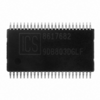
ICS9DB803DGLFT IDT, Integrated Device Technology Inc, ICS9DB803DGLFT Datasheet - Page 6

ICS9DB803DGLFT
Manufacturer Part Number
ICS9DB803DGLFT
Description
IC BUFFER 8OUTPUT DIFF 48-TSSOP
Manufacturer
IDT, Integrated Device Technology Inc
Type
Clock Bufferr
Datasheet
1.ICS9DB803DFLFT.pdf
(21 pages)
Specifications of ICS9DB803DGLFT
Input
HCSL
Output
HCSL, LVDS
Frequency - Max
400MHz
Voltage - Supply
3.135 V ~ 3.465 V
Operating Temperature
0°C ~ 70°C
Mounting Type
Surface Mount
Package / Case
48-TSSOP
Frequency-max
400MHz
Lead Free Status / RoHS Status
Lead free / RoHS Compliant
Other names
800-1252-2
9DB803DGLFT
9DB803DGLFT
Available stocks
Company
Part Number
Manufacturer
Quantity
Price
Part Number:
ICS9DB803DGLFT
Manufacturer:
ICS
Quantity:
20 000
Pin Description for OE_INV = 1
IDT
ICS9DB803D
Eight Output Differential Buffer for PCIe for Gen 2
TM
PIN #
/ICS
25
26
27
28
29
30
31
32
33
34
35
36
37
38
39
40
41
42
43
44
45
46
47
48
TM
Eight Output Differential Buffer for PCIe Gen 2
GND
PD
DIF_STOP
HIGH_BW#
DIF_4#
DIF_4
VDD
GND
DIF_5#
DIF_5
OE5#
OE6#
DIF_6#
DIF_6
VDD
OE_INV
DIF_7#
DIF_7
OE4#
OE7#
LOCK
IREF
GNDA
VDDA
PIN NAME
PIN TYPE
PWR
PWR
PWR
PWR
PWR
PWR
PWR
OUT
OUT
OUT
OUT
OUT
OUT
OUT
OUT
OUT
IN
IN
IN
IN
IN
IN
IN
IN
Ground pin.
Asynchronous active high input pin used to power down the device.
The internal clocks are disabled and the VCO is stopped.
Active High input to stop differential output clocks.
3.3V input for selecting PLL Band Width
0 = High, 1= Low
0.7V differential complement clock output
0.7V differential true clock output
Power supply, nominal 3.3V
Ground pin.
0.7V differential complement clock output
0.7V differential true clock output
Active low input for enabling DIF pair 5.
1 = tri-state outputs, 0 = enable outputs
Active low input for enabling DIF pair 6.
1 = tri-state outputs, 0 = enable outputs
0.7V differential complement clock output
0.7V differential true clock output
Power supply, nominal 3.3V
This latched input selects the polarity of the OE pins.
0 = OE pins active high, 1 = OE pins active low (OE#)
0.7V differential complement clock output
0.7V differential true clock output
Active low input for enabling DIF pair 4
1 = tri-state outputs, 0 = enable outputs
Active low input for enabling DIF pair 7.
1 = tri-state outputs, 0 = enable outputs
3.3V output indicating PLL Lock Status. This pin goes high when lock
is achieved.
This pin establishes the reference current for the differential current-
mode output pairs. This pin requires a fixed precision resistor tied to
ground in order to establish the appropriate current. 475 ohms is the
standard value.
Ground pin for the PLL core.
3.3V power for the PLL core.
6
DESCRIPTION
ICS9DB803D
REV J 01/27/11


