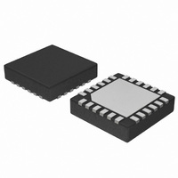
NB6L295MNG ON Semiconductor, NB6L295MNG Datasheet - Page 5

NB6L295MNG
Manufacturer Part Number
NB6L295MNG
Description
IC CLOCK/DATA DELAY 2CH 24-QFN
Manufacturer
ON Semiconductor
Type
Programmable Delay Chipr
Datasheet
1.NB6L295MNTXG.pdf
(14 pages)
Specifications of NB6L295MNG
Input
CML, LVDS, LVPECL
Output
CML
Frequency - Max
1.5GHz
Voltage - Supply
2.4 V ~ 3.6 V
Operating Temperature
-40°C ~ 85°C
Mounting Type
Surface Mount
Package / Case
24-TFQFN Exposed Pad
Frequency-max
1.5GHz
Function
Active Programmable Delay Line
Supply Voltage (min)
2.375 V
Maximum Operating Temperature
+ 85 C
Minimum Operating Temperature
- 40 C
Mounting Style
SMD/SMT
Supply Voltage (max)
3.6 V
Lead Free Status / RoHS Status
Lead free / RoHS Compliant
Available stocks
Company
Part Number
Manufacturer
Quantity
Price
Part Number:
NB6L295MNG
Manufacturer:
ON/安森美
Quantity:
20 000
NOTE: Device will meet the specifications after thermal equilibrium has been established when mounted in a test socket or printed circuit
5. LVPECL outputs loaded with 50 W to V
6. Input and output parameters vary 1:1 with V
7. V
8. V
9. V
Table 4. DC CHARACTERISTICS, MULTI−LEVEL INPUTS
+85°C
POWER SUPPLY CURRENT
LVPECL OUTPUTS (Notes 5 and 6, Figure 21)
DIFFERENTIAL INPUT DRIVEN SINGLE−ENDED (see Figures 10 and 11) (Note 7)
DIFFERENTIAL INPUTS DRIVEN DIFFERENTIALLY (see Figures 12 and 13) (Note 8)
SINGLE−ENDED LVCMOS/LVTTL CONTROL INPUTS
TERMINATION RESISTORS
Symbol
I
V
V
V
V
V
V
V
V
V
V
I
I
V
V
I
I
R
CC
IH
IL
IH
IL
OH
OL
th
IH
IL
ISE
IHD
ILD
ID
CMR
IH
IL
TIN
single−ended mode.
of the differential input signal.
th
IHD
CMR
, V
board with maintained transverse airflow greater than 500 lfpm. Electrical parameters are guaranteed only over the declared
operating temperature range. Functional operation of the device exceeding these conditions is not implied. Device specification limit
values are applied individually under normal operating conditions and not valid simultaneously.
, V
(min) varies 1:1 with voltage on GND Pin, V
IH
ILD,
, V
Power Supply Current (Inputs, V
I
Output HIGH Voltage
Output LOW Voltage
Input Threshold Reference Voltage Range
Single−Ended Input HIGH Voltage
Single−Ended Input LOW Voltage
Single−Ended Input Voltage Amplitude (V
Differential Input HIGH Voltage
Differential Input LOW Voltage
Differential Input Voltage Swing (INx, INx) (V
Input Common Mode Range (Differential Configuration) (Note 9)
Input HIGH Current INx/INx, (VTn/VTn Open)
Input LOW Current IN/INX, (VTn/VTn Open)
Single−Ended Input HIGH Voltage
Single−Ended Input LOW Voltage
Input HIGH Current
Input LOW Current
Internal Input Termination Resistor
CC0
IL,,
V
ID
, and I
and V
and V
CC1
ISE
CMR
)
parameters must be complied with simultaneously. V
parameters must be complied with simultaneously.
Characteristic
CC
Tx
− 2.0 V for proper operation.
and Outputs Open) (Sum of I
CC
.
CMR
IH
V
V
V
V
CC
CC
CC
CC
− V
IHD
(max) varies 1:1 with V
http://onsemi.com
= V
= V
= V
= V
IL
− V
)
CC0
CC0
CC0
CC0
ILD
= V
= V
= V
= V
)
5
V
CC1
CC1
CC1
CC1
CC
= V
= 3.3 V
= 2.5 V
= 3.3 V
= 2.5 V
CC
CC0
,
CC
th
= V
is applied to the complementary input when operating in
. The V
V
V
V
CC1
V
CC
CC
CC
th
2225
1425
1475
1050
GND
1200
GND
−150
−150
2000
GND
−150
−150
Min
675
300
150
950
110
= 2.375 V to 3.6 V, GND = 0 V, T
40
− 1075
− 1825
− 1825
+ 150
CMR
range is referenced to the most positive side
V
V
V
CC
CC
CC
2350
1550
1575
Typ
140
775
50
− 1725
− 1725
− 950
V
V
V
V
V
V
V
V
V
CC
CC
CC
CC
CC
CC
CC
th
CC
2475
1675
1675
Max
V
V
V
170
900
150
150
800
150
150
60
− 1625
− 1600
− 150
− GND
− GND
A
CC
CC
CC
− 825
− 150
− 150
– 75
= −40°C to
Unit
mA
mV
mV
mV
mV
mV
mV
mV
mV
mV
mV
mV
mV
mA
mA
mA
mA
W


