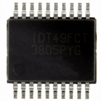
IDT49FCT3805PYG8 IDT, Integrated Device Technology Inc, IDT49FCT3805PYG8 Datasheet - Page 4

IDT49FCT3805PYG8
Manufacturer Part Number
IDT49FCT3805PYG8
Description
IC CLK BUFFER/DVR 1:5 20SSOP
Manufacturer
IDT, Integrated Device Technology Inc
Series
49FCTr
Type
Fanout Buffer (Distribution)r
Datasheet
1.IDT49FCT3805AQG8.pdf
(7 pages)
Specifications of IDT49FCT3805PYG8
Number Of Circuits
1
Ratio - Input:output
1:5
Differential - Input:output
No/No
Input
LVTTL
Output
LVTTL
Frequency - Max
166MHz
Voltage - Supply
3 V ~ 3.6 V
Operating Temperature
0°C ~ 70°C
Mounting Type
Surface Mount
Package / Case
20-SSOP
Frequency-max
166MHz
Number Of Outputs
10
Operating Supply Voltage (max)
3.6V
Operating Temp Range
0C to 70C
Propagation Delay Time
5.8ns
Operating Supply Voltage (min)
3V
Mounting
Surface Mount
Pin Count
20
Operating Supply Voltage (typ)
3.3V
Package Type
SSOP
Quiescent Current
10uA
Operating Temperature Classification
Commercial
Lead Free Status / RoHS Status
Lead free / RoHS Compliant
Other names
49FCT3805PYG8
800-1350-2
800-1350-2
NOTES:
1. For conditions shown as Max. or Min., use appropriate value specified under Electrical Characteristics for the applicable device type.
2. Typical values are at V
3. Per TTL driven input (V
4. This parameter is not directly testable, but is derived for use in Total Power Supply calculations.
5. Values for these conditions are examples of the I
6.
POWER SUPPLY CHARACTERISTICS
IDT49FCT3805/A
3.3V CMOS BUFFER/CLOCK DRIVER
I
I
I
∆I
D
N
I
f
N
All currents are in milliamps and all frequencies are in megahertz.
Symbol
C
C
CC
CCD
O
H
T
O
= I
CC
∆I
= I
I
= Output Frequency
CCD
= Number of TTL Inputs at D
= Number of Outputs at f
= Quiescent Current (I
= Duty Cycle for TTL Inputs High
I
C
CC
QUIESCENT
CC
= Dynamic Current Caused by an Input Transition Pair (HLH or LHL)
= Power Supply Current for a TTL High Input (V
+ ∆I
CC
+ I
D
H
INPUTS
N
T
Quiescent Power Supply Current
TTL Inputs HIGH
Dynamic Power Supply Current
Total Power Supply Current
+ I
CC
+ I
IN
CCD
CCL
DYNAMIC
= V
= 3.3V, +25°C ambient.
O
(f
, I
CC
O
Parameter
CCH
N
H
O
-0.6V); all other inputs at V
)
and I
CCZ
)
C
(6)
formula. These limits are guaranteed but not tested.
I
N
(4)
= V
CC
CC
-0.6V)
or GND.
V
V
V
Outputs Open
OE
Per Output Toggling
50% Duty Cycle
V
Outputs Open
f
50% Duty Cycle
OE
Mon. Output Toggling
V
Outputs Open
f
50% Duty Cycle
OE
Eleven Outputs Toggling
O
O
CC
IN
CC
CC
CC
= 25MHz
= 50MHz
A
A
A
= V
= Max.
= Max.
= Max.
= OE
= Max.
= OE
= OE
CC –
B
B
B
0.6V
= V
= GND
= GND
Test Conditions
(3)
CC
4
V
V
V
V
V
V
V
V
V
V
COMMERCIAL AND INDUSTRIAL TEMPERATURE RANGE
IN
IN
IN
IN
IN
IN
IN
IN
IN
IN
(1)
= V
= V
= V
= V
= V
= GND
= GND
= GND
= GND
= GND
CC
CC
CC –
CC
CC –
0.6V
0.6V
Min.
—
—
—
—
—
—
Typ.
0.035
0.9
0.9
10
20
20
(2)
Max.
0.06
33
33
1.6
1.6
30
(5)
(5)
mA/MHz
mA
Unit
µA


