SY89873LMG Micrel Inc, SY89873LMG Datasheet
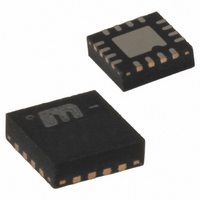
IC CLK DVDR ANY DIFF-LVDS 16MLF

SY89873LMG

Manufacturer Part Number
SY89873LMG
Description
IC CLK DVDR ANY DIFF-LVDS 16MLF
Manufacturer
Micrel Inc
Series
Precision Edge®r
Type
Fanout Buffer (Distribution), Dividerr
Datasheet

Specifications of SY89873LMG

Number Of Circuits
1
Ratio - Input:output
1:3
Differential - Input:output
Yes/Yes
Input
CML, HSTL, LVDS, LVPECL
Output
LVDS
Frequency - Max
2GHz
Voltage - Supply
2.97 V ~ 3.63 V
Operating Temperature
-40°C ~ 85°C
Mounting Type
Surface Mount
Package / Case
16-MLF®, QFN
Frequency-max
2GHz
Function
Clock Divider
Operating Temperature (max)
85C
Operating Temperature (min)
-40C
Package Type
MLF
Pin Count
16
Mounting
Surface Mount
Lead Free Status / RoHS Status
Lead free / RoHS Compliant
Other names
576-1436

Available stocks

Company
Part Number
Manufacturer
Quantity
Price
Part Number:
SY89873LMG
Manufacturer:
MICREL
Quantity:
436
Part Number:
SY89873LMG
Manufacturer:
MICREL/麦瑞
Quantity:
20 000
M9999-082407
hbwhelp@micrel.com or (408) 955-1690
Micrel, Inc.
Precision Edge is a registered trademark of Micrel, Inc.
Micro LeadFrame and MLF are registered trademarks of Amkor Technology, Inc.
FEATURES
APPLICATIONS
FUNCTIONAL BLOCK DIAGRAM
Guaranteed AC performance
• > 2.0GHz f
• > 3.0GHz f
• < 800ps t
• < 15ps within-device skew
• < 190ps rise/fall time
Low jitter design
• < 1ps
• < 10ps
Unique input termination and V
and AC-coupled inputs: any differential inputs
(LVPECL, LVDS, CML, HSTL)
Precision differential LVDS outputs
Matched delay: all outputs have matched delay,
independent of divider setting
TTL/CMOS inputs for select and reset/disable
Two LVDS output banks (matched delay)
• Bank A: Buffered copy of input clock (undivided)
• Bank B: Divided output (
3.3V power supply
Wide operating temperature range: –40
Available in 16-pin (3mm × × × × × 3mm) MLF
SONET/SDH line cards
Transponders
High-end, multiprocessor servers
V
REF-AC
two copies
/IN
S0
S1
IN
V
T
/RESET
RMS
50Ω
50Ω
PP
PD
Decoder
total jitter
cycle-to-cycle jitter
MAX
MAX
(matched-delay between banks)
output toggle
input
Enable
FF
÷
2,
Divided
Enable
2, 4, 8
MUX
or 16
by
÷
T
4,
pin for DC-coupled
÷
8,
3.3V, 2.0GHz ANY DIFF. IN-TO-LVDS
PROGRAMMABLE CLOCK DIVIDER
FANOUT BUFFER W/ INTERNAL TERMINATION
®
÷
16),
package
°
C to +85
QA
/QA
QB0
/QB0
QB1
/QB1
°
C
1
divider accepts any high-speed differential clock input (AC- or
DC-coupled) CML, LVPECL, HSTL or LVDS and divides down
the frequency using a programmable divider ratio to create a
frequency-locked, lower speed version of the input clock. The
SY89873L includes two output banks. Bank A is an exact
copy of the input clock (pass through) with matched
propagation delay to Bank B, the divided output bank. Available
divider ratios are 2, 4, 8 and 16. In a typical 622MHz clock
system this would provide availability of 311MHz, 155MHz,
77MHz or 38MHz auxiliary clock components.
design that allows access to the termination network through
a VT pin. This feature allows the device to easily interface to
all AC- or DC-coupled differential logic standards. A V
reference is included for AC-coupled applications.
Edge
consider the SY89872U. For applications that require an
LVPECL output, consider the SY89871U.
(Bank B). In the pass-through function (Bank A) the /RESET
synchronously enables or disables the outputs on the next
falling edge of IN (rising edge of /N). Refer to the Timing
Diagram.
site at: www.micrel.com.
DESCRIPTION
TYPICAL APPLICATION
This 3.3V low-skew, low-jitter, precision LVDS output clock
The differential input buffer has a unique internal termination
The SY89873L is part of Micrel’s high-speed Precision
The /RESET input asynchronously resets the divider outputs
All support documentation can be found on Micrel’s web
622MHz LVPECL
®
Clock In
timing and distribution family. For 2.5V applications,
/IN
Bank B: 155.5MHz: For OC-3 line card
Bank A: 622MHz: For OC-12 line card
IN
SONET Clock Generator
622MHz/155.5MHz
Set to pass-through
Set to divide-by-4
Clock Gen
OC-12 or
OC-3
Precision Edge
QA
/QA
QB
/QB
Rev.: F
Issue Date: February 2007
Precision Edge
Precision Edge
155.5MHz LVDS
SY89873L
622MHz LVDS
Clock Out
Clock Out
Amendment: /0
SY89873L
REF-AC
®
®
®

Related parts for SY89873LMG

SY89873LMG Summary of contents

Page 1

Micrel, Inc. FEATURES Guaranteed AC performance • > 2.0GHz f output toggle MAX • > 3.0GHz f input MAX • < 800ps t (matched-delay between banks) PD • < 15ps within-device skew • < 190ps rise/fall time Low jitter design ...

Page 2

... SY89873LMI MLF-16 (2) SY89873LMITR MLF-16 (3) SY89873LMG MLF-16 (2, 3) SY89873LMGTR MLF-16 Notes: 1. Contact factory for die availability. Dice are guaranteed Tape and Reel. 3. Pb-Free package is recommended for new designs. Pin Function Differential Buffered Output Clocks: Divide 16. LVDS compatible. Differential Buffered Undivided Output Clock: LVDS compatible. ...

Page 3

Micrel, Inc. Absolute Maximum Ratings Supply Voltage (V ) .................................. –0.5V to +4.0V CC Input Voltage (V ) .................................. –0. LVDS Output Current (I ) .................................... ±10mA OUT Input Current IN, / .......................................... ±50mA IN ...

Page 4

Micrel, Inc. LVDS OUTPUT DC ELECTRICAL CHARACTERISTICS V = 3.3V ±10 –40°C to +85°C; Unless otherwise stated Symbol Parameter V Output Voltage Swing OUT V Output High Voltage OH V Output Low Voltage OL V Output ...

Page 5

Micrel, Inc. AC ELECTRICAL CHARACTERISTICS V = 3.3V ±10 –40°C to +85°C; Unless otherwise stated Symbol Parameter f Maximum Output Toggle Frequency MAX (Bank A and Bank B) Maximum Input Frequency t Differential Propagation Delay PD ...

Page 6

Micrel, Inc. LVDS OUTPUT GND Figure 1a. LVDS Differential Measurement DEFINITION OF SINGLE-ENDED AND DIFFERENTIAL SWING 350mV (Typical) Figure 1c. Single-Ended Swing TIMING DIAGRAM /RESET /IN QB /QB QA /QA M9999-082407 hbwhelp@micrel.com ...

Page 7

Micrel, Inc. TYPICAL OPERATING CHARACTERISTICS V = 3.3V 400mV 25°C, unless otherwise stated Output Amplitude vs. Frequency 350 300 250 200 150 100 500 1000 1500 2000 2500 FREQUENCY (MHz) ...

Page 8

Micrel, Inc. FUNCTIONAL CHARACTERISTICS Conditions 3.3V 25°C, unless otherwise stated 622MHz and QB @ 155.5MHz (Divided-by-4) QA /QA 622MHz QB ÷4 /QB 155MHz TIME (1ns/div.) M9999-082407 hbwhelp@micrel.com or (408) 955-1690 QA Output ...

Page 9

Micrel, Inc. INPUT BUFFER STRUCTURE V CC 1.86kΩ 1.86kΩ IN 50Ω 50Ω GND /IN Figure 2a. Simplified Differential Input Stage M9999-082407 hbwhelp@micrel.com or (408) 955-1690 1.86kΩ 1.86kΩ Figure 2b. Simplified TTL/CMOS Input 9 Precision Edge SY89873L V CC ...

Page 10

Micrel, Inc. INPUT INTERFACE APPLICATIONS CML /IN SY89873L GND REF-AC Figure 3a. DC-Coupled CML Input Interface LVPECL ...

Page 11

Micrel, Inc. ® 16-PIN MicroLeadFrame Package Notes: 1. Package meets Level 2 moisture sensitivity classification, and is shipped in dry-pack form. 2. Exposed pads must be soldered to a ground for proper thermal management. MICREL, INC. 2180 FORTUNE DRIVE SAN ...

Related keywords