ICS8302AMLF IDT, Integrated Device Technology Inc, ICS8302AMLF Datasheet
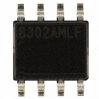
IC CLK FANOUT BUFFER 1:2 8SOIC

ICS8302AMLF

Manufacturer Part Number
ICS8302AMLF
Description
IC CLK FANOUT BUFFER 1:2 8SOIC
Manufacturer
IDT, Integrated Device Technology Inc
Series
HiPerClockS™r
Type
Fanout Buffer (Distribution)r
Datasheets

Specifications of ICS8302AMLF

Number Of Circuits
1
Ratio - Input:output
1:2
Differential - Input:output
No/No
Input
LVCMOS, LVTTL
Output
LVCMOS, LVTTL
Frequency - Max
200MHz
Voltage - Supply
3.135 V ~ 3.465 V
Operating Temperature
0°C ~ 70°C
Mounting Type
Surface Mount
Package / Case
8-SOIC
Frequency-max
200MHz
Number Of Outputs
2
Operating Supply Voltage (max)
3.465V
Operating Temp Range
0C to 70C
Propagation Delay Time
3.3ns
Operating Supply Voltage (min)
3.135V
Mounting
Surface Mount
Pin Count
8
Operating Supply Voltage (typ)
3.3V
Package Type
SOIC N
Duty Cycle
60%
Operating Temperature Classification
Commercial
Lead Free Status / RoHS Status
Lead free / RoHS Compliant
Other names
800-1104
800-1104-5
800-1104
8302AMLF

Available stocks

Company
Part Number
Manufacturer
Quantity
Price
Part Number:
ICS8302AMLF
Manufacturer:
NS/TI
Quantity:
4 500
Part Number:
ICS8302AMLF
Manufacturer:
ICS
Quantity:
20 000
B
G
The ICS8302 is a low skew, 1-to- 2 LVCMOS/LVTTL
Fanout Buffer. The ICS8302 hasa single ended clock input.
The single endedclock input accepts LVCMOS or LVTTL
input levels. The ICS8302 features a pair of LVCMOS/LVTTL
outputs. The ICS8302 is characterized at full 3.3V for
input V
supply modes (V
skew characteristics make the ICS8302 ideal for clock
distribution applications demanding well defined performance
and repeatibility.
8302AM
LOCK
ENERAL
DD
,and mixed 3.3V and 2.5V for output operating
CLK
D
IAGRAM
D
DDO
ESCRIPTION
). Guaranteed output and part-to-part
Q0
Q1
www.idt.com
1
F
• 2 LVCMOS / LVTTL outputs
• LVCMOS / LVTTL clock input accepts LVCMOS
• Maximum output frequency: 200MHz
• Output skew: 25ps (typical)
• Part-to-part skew: 250ps (typical)
• Small 8 lead SOIC package saves board space
• Full 3.3V or 3.3V core, 2.5V supply modes
• 0°C to 70°C ambient operating temperature
• Lead-Free package fully RoHS compliant
P
or LVTTL input levels
EATURES
IN
A
LVCMOS / LVTTL F
SSIGNMENT
3.8mm x 4.8mm, x 1.47mm package body
GND
V
CLK
V
DDO
DD
8-Lead SOIC
ICS8302
M Package
Top View
1
2
3
4
8
7
6
5
L
OW
Q0
GND
V
Q1
DDO
ANOUT
S
ICS8302
KEW
REV. D JULY 30, 2010
, 1-
B
UFFER
TO
-2

Related parts for ICS8302AMLF

ICS8302AMLF Summary of contents

Page 1

G D ENERAL ESCRIPTION The ICS8302 is a low skew, 1-to- 2 LVCMOS/LVTTL Fanout Buffer. The ICS8302 hasa single ended clock input. The single endedclock input accepts LVCMOS or LVTTL input levels. The ICS8302 features a pair of LVCMOS/LVTTL outputs. ...

Page 2

ABLE IN ESCRIPTIONS ...

Page 3

BSOLUTE AXIMUM ATINGS Supply Voltage Inputs, V -0. Outputs, V -0. Package Thermal Impedance, JA Storage Temperature, T -65°C to 150°C STG T 3A ABLE ...

Page 4

T 3C ABLE OWER UPPLY HARACTERISTICS ...

Page 5

P ARAMETER 1.65V± DDO LVCMOS GND -1.65V±5% 3. UTPUT OAD EST IRCUIT PART PART tsk(pp ART TO ...

Page 6

ABLE VS IR LOW ABLE FOR JA Single-Layer PCB, JEDEC Standard Test Boards Multi-Layer PCB, JEDEC Standard Test Boards NOTE: Most modern PCB designs use multi-layered boards. The data in the second ...

Page 7

ACKAGE UTLINE UFFIX FOR EAD T ABLE Reference Document: JEDEC Publication 95, MS-012 8302AM LVCMOS / LVTTL F SOIC ACKAGE IMENSIONS ...

Page 8

ABLE RDERING NFORMATION ...

Page 9

& ...

Page 10

We’ve Got Your Timing Solution. 6024 Silver Creek Valley Road San Jose, CA 95138 © 2010 Integrated Device Technology, Inc. All rights reserved. Product specifications subject to change without notice. IDT, the IDT logo, ICS and HiPerClockS are trademarks of ...

Related keywords