CY29946AXI Cypress Semiconductor Corp, CY29946AXI Datasheet - Page 3
CY29946AXI
Manufacturer Part Number
CY29946AXI
Description
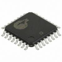
IC CLK BUFF 1:10 200MHZ 32TQFP
Manufacturer
Cypress Semiconductor Corp
Type
Fanout Buffer (Distribution), Divider, Multiplexerr
Datasheet
1.CY29946AXC.pdf
(6 pages)
Specifications of CY29946AXI
Package / Case
32-TQFP
Number Of Circuits
1
Ratio - Input:output
2:10
Differential - Input:output
No/Yes
Input
LVCMOS, LVTTL
Output
LVCMOS, LVTTL
Frequency - Max
200MHz
Voltage - Supply
2.375 V ~ 3.63 V
Operating Temperature
-40°C ~ 85°C
Mounting Type
Surface Mount
Frequency-max
200MHz
Minimum Operating Temperature
- 40 C
Mounting Style
SMD/SMT
Multiply / Divide Factor
1:10
Number Of Clock Inputs
2
Output Logic Level
LVCMOS, LVTTL
Supply Voltage (max)
3.63 V
Supply Voltage (min)
2.375 V
Maximum Operating Temperature
+ 85 C
Lead Free Status / RoHS Status
Lead free / RoHS Compliant
Lead Free Status / RoHS Status
Lead free / RoHS Compliant, Lead free / RoHS Compliant
Available stocks
Company
Part Number
Manufacturer
Quantity
Price
Company:

Part Number:
CY29946AXI
Manufacturer:
Cypress
Quantity:
228
Company:
Part Number:
CY29946AXI
Manufacturer:
Cypress Semiconductor Corp
Quantity:
10 000
Part Number:
CY29946AXI
Manufacturer:
CYPRESS/赛普拉斯
Quantity:
20 000
Company:
Part Number:
CY29946AXIT
Manufacturer:
Cypress Semiconductor Corp
Quantity:
10 000


Document #: 38-07286 Rev. *E
Absolute Maximum Conditions
Maximum Input Voltage Relative to V
Maximum Input Voltage Relative to V
Storage Temperature: ................................ –65°C to + 150°C
Operating Temperature: ................................ –40°C to +85°C
Maximum ESD protection ............................................... 2 kV
Maximum Power Supply: ................................................5.5V
Maximum Input Current: ...........................................± 20 mA
DC Electrical Specifications:
AC Electrical Specifications
Notes:
V
V
I
I
V
V
I
I
Z
C
Fmax
Tpd
FoutDC
tpZL, tpZH
tpLZ, tpHZ
Tskew
Tskew(pp)
Tr/Tf
2. Multiple Supplies: The voltage on any input or I/O pin cannot exceed the power pin during power-up. Power supply sequencing is NOT required.
3. Inputs have pull-up/pull-down resistors that effect input current.
4. Driving series or parallel terminated 50Ω (or 50Ω to V
5. Parameters are guaranteed by design and characterization. Not 100% tested in production. All parameters specified with loaded outputs.
6. Outputs driving 50Ω transmission lines.
7. 50% input duty cycle.
8. See Figure 1.
9. Part-to-Part skew at a given temperature and voltage.
Parameter
IL
IH
DDQ
DD
Parameter
Out
IL
IH
OL
OH
in
Input Low Voltage
Input High Voltage
Input Low Current
Input High Current
Output Low Voltage
Output High Voltage
Quiescent Supply Current
Dynamic Supply Current
Output Impedance
Input Capacitance
Input Frequency
TTL_CLK To Q Delay
Output Duty Cycle
Output enable time (all outputs)
Output disable time (all outputs)
Output-to-Output Skew
Part-to-Part Skew
Output Clocks Rise/Fall Time
Description
Description
[6]
[3]
[9]
[3]
[6, 7]
[4]
[4]
[6]
SS
DD
V
[6, 8]
V
DD
: ............ V
: ............. V
DD
[2]
= V
= V
[8]
I
I
I
V
V
V
V
V
V
OL
OH
OH
DD
DD
DD
DD
DD
DD
DD
DDC
DDC
/2) transmission lines.
= 20 mA
= –20 mA, V
= –20 mA, V
= 3.3V, Outputs @ 100 MHz, CL = 30 pF
= 3.3V, Outputs @ 160 MHz, CL = 30 pF
= 2.5V, Outputs @ 100 MHz, CL = 30 pF
= 2.5V, Outputs @ 160 MHz, CL = 30 pF
= 3.3V
= 2.5V
V
V
Measured at V
0.8V to 2.0V,
V
0.6V to 1.8V,
V
DD
DD
DD
DD
= 3.3V ±10% or 2.5V ±5%, over the specified temperature range
DD
SS
= 3.3V ±10% or 2.5V ±5%, over the specified temperature range
= 3.3V
= 2.5V
= 3.3V
= 2.5V
– 0.3V
+ 0.3V
Conditions
DD
DD
Conditions
DD
= 3.3V
= 2.5V
This device contains circuitry to protect the inputs against
damage due to high static voltages or electric field; however,
precautions should be taken to avoid application of any
voltage higher than the maximum rated voltages to this circuit.
For proper operation, V
range:
V
Unused inputs must always be tied to an appropriate logic
voltage level (either V
/2
SS
< (V
in
or V
Min.
0.10
0.10
5.0
45
out
2
2
) < V
SS
DD
in
and V
or V
.
Typ.
150
2.0
Min.
V
2.0
2.5
1.8
12
14
DD
SS
out
).
should be constrained to the
Typ.
130
225
160
95
15
18
5
4
Max.
11.5
200
170
250
4.5
1.0
1.3
55
10
10
[5]
CY29946
Max.
–100
V
100
0.8
0.4
18
22
7
DD
Page 3 of 6
MHz
Unit
ns
ns
ns
ps
ns
ns
%
Unit
mA
mA
µA
µA
pF
W
V
V
V
V
[+] Feedback
Related parts for CY29946AXI
Image
Part Number
Description
Manufacturer
Datasheet
Request
R

Part Number:
Description:
Manufacturer:
Cypress Semiconductor Corp
Datasheet:
Part Number:
Description:
Manufacturer:
Cypress Semiconductor Corp
Datasheet:
Part Number:
Description:
Manufacturer:
Cypress Semiconductor Corp
Datasheet:
Part Number:
Description:
Manufacturer:
Cypress Semiconductor Corp
Datasheet:
Part Number:
Description:
Manufacturer:
Cypress Semiconductor Corp
Datasheet: