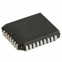
CY7B991V-2JXC Cypress Semiconductor Corp, CY7B991V-2JXC Datasheet - Page 12

CY7B991V-2JXC
Manufacturer Part Number
CY7B991V-2JXC
Description
IC CLK BUFF SKEW 8OUT 32PLCC
Manufacturer
Cypress Semiconductor Corp
Type
Buffer/Driverr
Series
RoboClock™r
Datasheet
1.CY7B991V-7JXC.pdf
(17 pages)
Specifications of CY7B991V-2JXC
Number Of Circuits
1
Package / Case
32-PLCC
Ratio - Input:output
8:8
Differential - Input:output
Yes/Yes
Input
3-State
Output
LVTTL
Frequency - Max
80MHz
Voltage - Supply
2.97 V ~ 3.63 V
Operating Temperature
0°C ~ 70°C
Mounting Type
Surface Mount
Frequency-max
80MHz
Output Frequency Range
3.75 MHz to 80 MHz
Supply Voltage (max)
3.63 V
Supply Voltage (min)
2.97 V
Maximum Operating Temperature
+ 70 C
Minimum Operating Temperature
0 C
Mounting Style
SMD/SMT
Operating Supply Voltage
3.3 V
Lead Free Status / RoHS Status
Lead free / RoHS Compliant
Lead Free Status / RoHS Status
Lead free / RoHS Compliant, Lead free / RoHS Compliant
Other names
428-1718-5
Available stocks
Company
Part Number
Manufacturer
Quantity
Price
Company:
Part Number:
CY7B991V-2JXC
Manufacturer:
Cypress Semiconductor Corp
Quantity:
10 000
Company:
Part Number:
CY7B991V-2JXCT
Manufacturer:
Cypress Semiconductor Corp
Quantity:
10 000
Switching Characteristics
Over the Operating Range
Document Number: 38-07141 Rev. *G
f
t
t
t
t
t
t
t
t
t
t
t
t
t
t
t
t
t
t
NOM
RPWH
RPWL
U
SKEWPR
SKEW0
SKEW1
SKEW2
SKEW3
SKEW4
DEV
PD
ODCV
PWH
PWL
ORISE
OFALL
LOCK
JR
Parameter
Operating clock
Frequency in MHz
REF pulse width HIGH
REF pulse width LOW
Programmable skew unit
Zero output matched pair skew (XQ0, XQ1)
Zero output skew (All Outputs)
Output skew (rise-rise, fall-fall, same class outputs)
Output skew (rise-fall, nominal-inverted, divided-divided)
Output skew (rise-rise, fall-fall, different class outputs)
Output skew (rise-fall, nominal-divided, divided-inverted)
Device-to-device skew
Propagation delay, REF rise to FB rise
Output duty cycle variation
Output HIGH time deviation from 50%
Output LOW time deviation from 50%
Output rise time
Output fall time
PLL lock time
Cycle-to-cycle output jitter
[2, 10]
[21]
[19, 20]
[19, 20]
[12, 18]
–
7 Option
[18]
Description
[13, 15]
[19]
[19]
FS = LOW
FS = MID
FS = HIGH
RMS
Peak-to-peak
[13, 14]
[11]
[1, 2]
[12, 16]
[1, 2]
[1, 2]
[13, 17]
[11]
[13, 17]
[13, 17]
–0.7
–1.2
0.15
0.15
Min
5.0
5.0
15
25
40
–
–
–
–
–
–
–
–
–
–
–
–
CY7B991V–7
Typ
0.1
0.3
0.6
1.0
0.7
1.2
0.0
0.0
1.5
1.5
–
–
–
–
–
–
–
–
–
–
–
See
Table 2
Max
0.25
0.75
1.65
+0.7
+1.2
200
1.0
1.5
1.2
1.7
3.5
2.5
2.5
0.5
30
50
80
25
–
–
3
CY7B991V
Page 12 of 17
MHz
Unit
ms
ns
ns
ns
ns
ns
ns
ns
ns
ns
ns
ns
ns
ns
ns
ns
ps
ps
[+] Feedback


