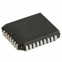
CY7B991-5JXI Cypress Semiconductor Corp, CY7B991-5JXI Datasheet - Page 14

CY7B991-5JXI
Manufacturer Part Number
CY7B991-5JXI
Description
IC CLK BUFF SKEW 8OUT 32PLCC
Manufacturer
Cypress Semiconductor Corp
Type
Buffer/Driverr
Series
RoboClock™r
Datasheet
1.CY7B991-7JXC.pdf
(20 pages)
Specifications of CY7B991-5JXI
Number Of Circuits
1
Package / Case
32-PLCC
Ratio - Input:output
8:8
Differential - Input:output
Yes/Yes
Input
3-State, TTL
Output
TTL
Frequency - Max
80MHz
Voltage - Supply
4.5 V ~ 5.5 V
Operating Temperature
-40°C ~ 85°C
Mounting Type
Surface Mount
Frequency-max
80MHz
Output Frequency Range
3.75 MHz to 80 MHz
Supply Voltage (max)
5.5 V
Supply Voltage (min)
4.5 V
Maximum Operating Temperature
+ 85 C
Minimum Operating Temperature
- 40 C
Mounting Style
SMD/SMT
Operating Supply Voltage
5 V
Lead Free Status / RoHS Status
Lead free / RoHS Compliant
Lead Free Status / RoHS Status
Lead free / RoHS Compliant, Lead free / RoHS Compliant
Available stocks
Company
Part Number
Manufacturer
Quantity
Price
Company:
Part Number:
CY7B991-5JXI
Manufacturer:
Cypress Semiconductor Corp
Quantity:
10 000
Part Number:
CY7B991-5JXI
Manufacturer:
CYPRESS/赛普拉斯
Quantity:
20 000
Company:
Part Number:
CY7B991-5JXIT
Manufacturer:
Cypress Semiconductor Corp
Quantity:
10 000
Part Number:
CY7B991-5JXIT
Manufacturer:
CYPRESS/赛普拉斯
Quantity:
20 000
the FB and REF inputs and aligns their rising edges to ensure
that all outputs have precise phase alignment.
Clock skews are advanced by ±6 time units (tU) when using an
output selected for zero skew as the feedback. A wider range of
delays is possible if the output connected to FB is also skewed.
Since “Zero Skew”, +tU, and –tU are defined relative to output
groups, and since the PLL aligns the rising edges of REF and
FB, you can create wider output skews by proper selection of the
xFn inputs. For example, a +10 tU between REF and 3Qx is
achieved by connecting 1Q0 to FB and setting 1F0 = 1F1 = GND,
3F0 = MID, and 3F1 = High. (Since FB aligns at –4 tU and 3Qx
skews to +6 tU, a total of +10 tU skew is realized.) Many other
configurations are realized by skewing both the outputs used as
the FB input and skewing the other outputs.
Figure 6. Inverted Output Connections
Figure 6
In this example the 4Q0 output used as the FB input is
programmed for invert (4F0 = 4F1 = HIGH) while the other three
pairs of outputs are programmed for zero skew. When 4F0 and
4F1 are tied high, 4Q0 and 4Q1 become inverted zero phase
outputs. The PLL aligns the rising edge of the FB input with the
rising edge of the REF. This causes the 1Q, 2Q, and 3Q outputs
to become the “inverted” outputs with respect to the REF input.
It is possible to have 2 inverted and 6 non-inverted outputs or 6
inverted and 2 non-inverted outputs by selecting the output
connected to FB. The correct configuration is determined by the
need for more (or fewer) inverted outputs. 1Q, 2Q, and 3Q
outputs can also be skewed to compensate for varying trace
delays independent of inversion on 4Q.
Document Number: 38-07138 Rev. *E
shows an example of the invert function of the PSCB.
FB
REF
FS
4F0
4F1
3F0
3F1
2F0
2F1
1F0
1F1
TEST
4Q0
4Q1
3Q0
3Q1
2Q0
2Q1
1Q0
1Q1
REF
F
Figure 7. Frequency Multiplier with Skew Connectrions
Figure 7
3Q0 output is programmed to divide by four and is sent to FB.
This causes the PLL to increase its frequency until the 3Q0 and
3Q1 outputs are locked at 20 MHz while the 1Qx and 2Qx
outputs run at 80 MHz. The 4Q0 and 4Q1 outputs are
programmed to divide by two, that results in a 40 MHz waveform
at these outputs. Note that the 20 and 40 MHz clocks fall simul-
taneously and are out of phase on their rising edge. This enables
the designer to use the rising edges of the
frequency outputs without concern for rising edge skew. The
2Q0, 2Q1, 1Q0, and 1Q1 outputs run at 80 MHz and are skewed
by programming their select inputs accordingly. Note that the FS
pin is wired for 80 MHz operation because that is the frequency
of the fastest output.
Figure 8. Frequency Divider Connections
Figure 8
2Q0 is fed back to the FB input and programmed for zero skew.
3Qx is programmed to divide by four. 4Qx is programmed to
divide by two. Note that the falling edges of the 4Qx and 3Qx
outputs are aligned. This enables the use of rising edges of the
1
mismatch. The 1Qx outputs are programmed to zero skew and
are aligned with the 2Qx outputs. In this example, the FS input
is grounded to configure the device in the 15 MHz to 30 MHz
⁄
2
20 MHz
20 MHz
frequency and
shows the PSCB configured as a clock multiplier. The
demonstrates the PSCB in a clock divider application.
FB
REF
FS
4F0
4F1
3F0
3F1
2F0
2F1
1F0
1F1
TEST
FB
REF
FS
4F0
4F1
3F0
3F1
2F0
2F1
1F0
1F1
TEST
1
⁄
4
4Q0
4Q1
3Q0
3Q1
2Q0
2Q1
1Q0
1Q1
4Q0
4Q1
3Q0
3Q1
2Q0
2Q1
1Q0
1Q1
frequency without concern for skew
REF
REF
1
⁄
2
frequency and
40 MHz
20 MHz
80 MHz
CY7B991
CY7B992
Page 14 of 20
10 MHz
20 MHz
5 MHz
1
⁄
4
[+] Feedback


