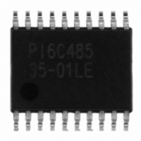
PI6C48535-01LE Pericom Semiconductor, PI6C48535-01LE Datasheet - Page 4

PI6C48535-01LE
Manufacturer Part Number
PI6C48535-01LE
Description
IC CLOCK BUFFER 20-TSSOP
Manufacturer
Pericom Semiconductor
Type
Fanout Buffer (Distribution), Multiplexerr
Datasheet
1.PI6C48535-01LE.pdf
(5 pages)
Specifications of PI6C48535-01LE
Number Of Circuits
1
Ratio - Input:output
2:4
Differential - Input:output
No/Yes
Input
LVCMOS, LVTTL
Output
LVPECL
Frequency - Max
500MHz
Voltage - Supply
3 V ~ 3.6 V
Operating Temperature
-40°C ~ 85°C
Mounting Type
Surface Mount
Package / Case
20-TSSOP
Frequency-max
500MHz
Output Logic Level
LVPECL
Supply Voltage (max)
3.6 V
Supply Voltage (min)
3 V
Maximum Operating Temperature
+ 85 C
Max Output Freq
500 MHz
Minimum Operating Temperature
- 40 C
Mounting Style
SMD/SMT
Number Of Clock Inputs
2
Number Of Outputs
16
Supply Current
60 mA
Lead Free Status / RoHS Status
Lead free / RoHS Compliant
Available stocks
Company
Part Number
Manufacturer
Quantity
Price
Company:
Part Number:
PI6C48535-01LE
Manufacturer:
Pericom
Quantity:
5 469
Part Number:
PI6C48535-01LEX
Manufacturer:
PERICOM
Quantity:
20 000
LVCMOS/LVTTL DC Characteristics
LVPECL DC Characteristics
Notes:
1.
AC Characteristics
Notes:
1. Measured from the V
2. Defined as skew between outputs at the same supply voltage and with equal load condition. Measured at the outputs differential crossing point.
3. Defined as skew between outputs on different parts operating at the same supply voltage and with equal load condition. Measured at the
4. All parameters are measured at 500 MHz unless noted otherwise
V
Symbol
Symbol
Symbol
T
outputs differential crossing point.
T
V
SWING
V
f
V
V
sk(pp)
odc
J
t
I
t
sk(o)
I
max
r
add
IH
Pd
IL
OH
OL
/t
IH
IL
f
11-0040
Outputs terminated with 50Ω to V
Input High
Input High
Input Low
Input Low
Peak-to-peak Output Voltage Swing
Voltage
Voltage
Current
Current
Output-to-output Skew
Output Rise/Fall time
Propagation Delay
Part-to-part Skew
Output Duty Cycle
CC
Output Frequency
Output High Voltage
Output Low Voltage
(T
Additive Jitter
/2 of the input to the differential output crossing point
Parameter
A
= -40
Parameter
Parameter
CLK0, CLK1, CLK_SEL
CLK
CLK
o
C to 85
CLK_EN, CLK_SEL
(T
0
0
CLK
, CLK
, CLK
CC
A
(3)
CLK_SEL
(1)
CLK_EN
CLK_EN
= -40
o
-2.0V
C, V
(2)
0
(1)
(1)
, CLK
1
1
, CLK_SEL
CC
, CLK_EN,
o
C to 85
= 3.0V to 3.6V)
(T
1
A
At 155.25MHz
over 12kHz to 20MHz
= -40
o
C, V
o
C to 85
Conditions
20% - 80%
CC
V
V
= 3.0V to 3.6V unless otherwise stated below.)
IN
IN
V
V
4
Conditions
o
IN
IN
C, V
= 0V, V
= 0V, V
Conditions
= V
= V
CC
CC
CC
LVTTL/LVCMOS to LVPECL Fanout Buffer
= 3.0V to 3.6V unless otherwise stated below.)
CC
CC
= 3.6V
= 3.6V
= 3.6V
= 3.6V
Min.
1.0
80
40
V
V
Min.
CC
CC
Min.
0.6
-150
-0.3
-0.3
-5
2
-1.4
-2.0
Typ.
36.7
Typ.
Typ.
3.3V Low Skew 1-to-4
Max.
V
V
V
500
150
400
1.9
80
60
Max.
Max.
CC
CC
CC
150
1.0
1.3
0.8
PI6C48535-01
5
+0.3
-0.9
-1.7
PS8735A
Units
MHz
Units
Units
ns
ps
%
fs
uA
uA
uA
uA
V
V
V
V
03/25/11


