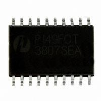
PI49FCT3807ASE Pericom Semiconductor, PI49FCT3807ASE Datasheet - Page 3

PI49FCT3807ASE
Manufacturer Part Number
PI49FCT3807ASE
Description
IC 10-OUTPUT CLOCK DRV 20SOIC
Manufacturer
Pericom Semiconductor
Series
49FCTr
Type
Fanout Buffer (Distribution)r
Datasheet
1.PI49FCT3807CQE.pdf
(8 pages)
Specifications of PI49FCT3807ASE
Number Of Circuits
1
Ratio - Input:output
1:10
Differential - Input:output
No/No
Input
CMOS, TTL
Output
CMOS, TTL
Frequency - Max
66MHz
Voltage - Supply
3 V ~ 3.6 V
Operating Temperature
-40°C ~ 85°C
Mounting Type
Surface Mount
Package / Case
20-SOIC
Frequency-max
66MHz
Number Of Outputs
10
Operating Supply Voltage (max)
3.6V
Operating Temp Range
-40C to 85C
Propagation Delay Time
4ns
Operating Supply Voltage (min)
3V
Mounting
Surface Mount
Pin Count
20
Operating Supply Voltage (typ)
3.3V
Package Type
SOIC
Quiescent Current
3uA
Power Dissipation
500mW
Operating Temperature Classification
Industrial
Lead Free Status / RoHS Status
Lead free / RoHS Compliant
Power Supply Characteristics
Notes:
1.
2.
3.
4.
5.
Capacitance
Notes:
1.
Maximum Switching Characteristics
Notes:
1.
2.
3.
I
ΔI
I
C
C
t
t
t
t
F
CC
CCD
PLH
PHL
SK(O)
SK(P)
Symbol
Parameters
Parameters
IN
IN
OUT
CC
Other loading condition is described on page 4, “Test Circuits for All Outputs.”
These parameters are guaranteed by design.
Minimum propagation delay of 1.5ns is guaranteed by design.
For Max. or Min. conditions, use appropriate value specifi ed under Electrical Characteristics for the applicable device.
Typical values are at V
Per TTL driven input (V
This parameter is not directly testable, but is derived for use in Total Power Supply Calculations.
Values for these conditions are examples of the I
This parameter is determined by device characterization but is not production tested.
09-0005
Propagation Delay A to B
Skew between two outputs
of same package
Skew between opposite tran-
sitions of the same output
(t
Skew between outputs of
different packages at the
same power supply, temp.
and speed grade
PHL
(1)
(T
Quiescent Power
Supply Current
Supply Current per
Inputs @ TTL HIGH
Supply Current per
Input per MHz
A
- t
Input Capacitance
Output Capacitance
= 25°C, f = 1 MHz)
PHL
Description
De scrip tion
)
CC
(3)
IN
= 3.3V, +25°C ambient.
(3)
= V
(3)
(4)
CC
– 0.6V); all other inputs at V
De scrip tion
N
Conditions
R
V
V
V
Outputs Open
Per Output Toggling
50% Duty Cycle
C
L
L
CC
CC
CC
(Over operating range)
Test
= 500Ω
= 15pF
C
= Max.
= Max.
= Max.,
formula. These limits are guaranteed but not tested.
Test Conditions
Min. Max. Min. Max. Min. Max. Min. Max.
1.5
CC
Com.
3807
or GND.
3
4.5
0.5
0.5
1.0
V
or V
V
0.6V
V
V
(1)
IN
IN
IN
IN
Test Conditions
CC
= GND
= V
= V
= GND
1.5
(3)
V
V
3087A
Com.
OUT
CC
CC
IN
= 0V
= 0V
4.0
0.5
0.5
1.0
Min.
1.5
—
—
—
3087B
Com.
3.3V Fast CMOS Clock Driver
0.35
0.75
3.8
0.5
Typ
2.0
Typ
4.5
5.5
3
(2)
1.5
3807C
Com.
Max.
0.35
0.75
Max.
300
3.5
0.5
30
6.0
8.0
PI49FCT3807
PS7010F
Units
Units
MHz
Units
ns
mA/
μA
pF
11/16/09


