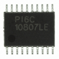
PI6C10807LE Pericom Semiconductor, PI6C10807LE Datasheet - Page 2

PI6C10807LE
Manufacturer Part Number
PI6C10807LE
Description
IC CLOCK BUFF NETW 20TSSOP
Manufacturer
Pericom Semiconductor
Type
Fanout Buffer (Distribution)r
Datasheet
1.PI6C10807LE.pdf
(7 pages)
Specifications of PI6C10807LE
Number Of Circuits
1
Ratio - Input:output
1:10
Differential - Input:output
No/No
Input
LVCMOS, LVTTL
Output
LVCMOS, LVTTL
Frequency - Max
250MHz
Voltage - Supply
1.65 V ~ 2.7 V
Operating Temperature
-40°C ~ 85°C
Mounting Type
Surface Mount
Package / Case
20-TSSOP
Frequency-max
250MHz
Number Of Outputs
10
Operating Supply Voltage (max)
2.7V
Operating Temp Range
-40C to 85C
Propagation Delay Time
2ns
Operating Supply Voltage (min)
1.65V
Mounting
Surface Mount
Pin Count
20
Operating Supply Voltage (typ)
1.8/2.5V
Package Type
TSSOP
Quiescent Current
10uA
Input Frequency
250MHz
Duty Cycle
57.5%
Operating Temperature Classification
Industrial
Lead Free Status / RoHS Status
Lead free / RoHS Compliant
2.5V Absolute Maximum Ratings
2.5V DC Characteristics
Notes:
1.
2.5V AC Characteristics
Notes:
4.
5.
2. Typical values are at V
1. See test circuit and waveforms.
2. Minimum limits are guaranteed but not tested on Propagation Delays.
3. Skew measured at worst case temperature (max. temp).
Parameters Description
Storage Temperature ...........................................................–65°C to +150°C
V
Output Voltage (max. 3.6V) .......................................... –0.5V to V
Input Voltage (max 3.6V) .............................................. –0.5V to V
t
DD
Parameters
PLH,
For Max. or Min. conditions, use appropriate operating range values.
Identical conditions: loading, transitions, supply voltage, temperature, package type and speed grade.
Outputs are measured at V
V
V
V
t
t
V
t
V
SK(O)
t
SK(P)
SK(T)
t
I
dc_out
Voltage ..........................................................................–0.5V to +3.6V
DD
OH
OL
dc_in
IH
IL
I
t
F
R
09-0084
t
IN
/t
PHL
F
3. 5
3, 5
3, 5
5
5
2, 5
Supply Voltage
Input HIGH Voltage
Input LOW Voltage
Input Current
Output High Voltage
Output LOW Voltage
De scrip tion
Input Frequency
CLKn Rise/Fall Time
Pulse Skew between opposite transitions
(t
Propagation Delay BUF_IN to CLKn
Output to Output Skew between any two
outputs of the same device @ same transition
Part to Part Skew between two identical out-
puts of different parts on the same board
Duty Cycle In @ Ins edge rate
Duty Cycle Out
PHL
DD
-t
PLH
= 2.5V, +25°C ambient and maximum loading.
DD
) of the same output
/2
(Over Operating Range: V
(Over Operating Range: V
V
V
V
DD
(Above which the useful life may be impaired. For user guidelines only, not tested.)
DD
DD
= Max, Vin = V
= Min., V
= Min., V
Logic HIGH level
Logic LOW level
Test Conditions
IN
IN
DD
DD
= V
- V
4
= 2.5V ± 0.2V, T
= 2.5V ± 0.2V, T
DD
IH
IH
or GND
2
or V
or V
DD
DD
1.8V/2.5V, 250MHz, 1:10 Networking Clock Buffer
C
C
Test Conditions
+0.5V
+0.5V
IL
L
L
IL
= 5pF, 125 MHz
= 5pF, 125 MHz
20% to 80%
Vin > V
1
I
I
I
I
I
I
OH
OH
OH
OL
OL
OL
A
A
= -40° to 85°C)
= -40° to 85°C)
= -1mA
= -2mA
= -8mA
Note: Stresses greater than those listed under MAXI-
MUM RAT INGS may cause permanent damage to the
device. This is a stress rating only and functional op er a tion
of the device at these or any other con di tions above those
indicated in the operational sec tions of this spec i fi ca tion is
not implied. Ex po sure to absolute maximum rating con di-
tions for extended periods may affect re li abil i ty.
= 1mA
= 2mA
= 8mA
DD
1
Min.
Min.
-0.3
1.0
2.3
1.7
2.0
1.7
1.7
45
40
0
Typ.
Typ
100
1.5
2.5
2
PS8862L
Max.
57.5
250
200
300
Max.
1.0
2.0
60
55
2.7
3.6
0.7
0.1
0.2
0.2
15
PI6C10807
Units
MHz
Units
ns
ps
ns
ps
%
05/01/09
μA
V
V


