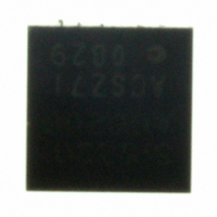
SI5330A-A00200-GM Silicon Laboratories Inc, SI5330A-A00200-GM Datasheet

SI5330A-A00200-GM
Specifications of SI5330A-A00200-GM
Available stocks
Related parts for SI5330A-A00200-GM
SI5330A-A00200-GM Summary of contents
Page 1
Features Supports single-ended or differential input clock ...
Page 2
... Si5330 1. Functional Block Diagrams Based on Orderable Part Number 1:4 Differential to Differential Buffer Si5330A/B/C IN1 IN2 IN3 LOS Control OEB 1:8 Differential to Single-Ended Buffer Si5330G/H/J IN1 IN2 IN3 LOS Control OEB Figure 1. Si5330 Functional Block Diagrams *Note: See Table 10 for detailed ordering information. ...
Page 3
T C ABLE O F ONTENTS Section 1. Functional Block Diagrams Based on Orderable Part Number Electrical Specifications . . ...
Page 4
Si5330 2. Electrical Specifications Table 1. Recommended Operating Conditions (V = 1.8 V –5% to +10%, 2.5 V ±10%, or 3.3 V ±10 Parameter Symbol Ambient Temperature Core Supply Voltage DD Output Buffer Supply V ...
Page 5
Table 3. DC Characteristics (V = 1.8 V –5% to +10%, 2.5 V ±10%, or 3.3 V ±10 Parameter Core Supply Current Output Buffer Supply Current Table 4. Thermal Characteristics Parameter Symbol Thermal Resistance JA Junction to ...
Page 6
Si5330 Table 6. Input and Output Clock Characteristics (V = 1.8 V –5% to +10%, 2.5 V ±10%, or 3.3 V ±10 Parameter Symbol Input Clock (AC Coupled Differential Input Clocks on Pin IN1/2) f Frequency IN V ...
Page 7
Table 6. Input and Output Clock Characteristics (Continued 1.8 V –5% to +10%, 2.5 V ±10%, or 3.3 V ±10 Parameter Symbol CMOS 20%-80 Rise/Fall Time CMOS 20%-80 ...
Page 8
Si5330 Table 7. OEB Input Specifications Parameter Symbol V Input Voltage Low IL V Input Voltage High IH R Input Resistance IN Table 8. Jitter Specifications (V = 1.8 V –5% to +10%, 2.5 V ±10%, or 3.3 V ±10%, ...
Page 9
Functional Description The Si5330 is a low-jitter, low-skew fanout buffer optimized for high-performance PCB clock distribution applications. The device produces four differential or eight single-ended, low-jitter output clocks from a single input clock. The input can accept either a ...
Page 10
... These pins are not used. Leave IN1 unconnected and IN2 connected to ground. Si5330F/K/L/M Single-Ended Devices. This is the single-ended clock input. Refer to AN408 for interfacing and termination details. Multi Si5330A/B/C/G/H/J Differential Input Devices. This pin is not used. Connect to ground. Ground. Must be connected to system ground. Ground. Must be connected to system ground. ...
Page 11
... Loss of Signal Indicator CLKIN present. Open Drain 1 = Loss of signal (LOS). This pin requires an external 1 kpull-up resistor. Si5330A/B/C/K/L/M Differential Output Devices. This is the negative side of the differential CLK3 output. Refer to AN408 for interfacing and termination details. Leave unconnected when not in use. Multi Si5330F/G/H/J Single-Ended Output Devices ...
Page 12
... Supply voltage for CLK1A,B. Use a 0.1 µF bypass cap Supply as close as possible to this pin. If CLK1 is not used, this pin must be tied to V Si5330A/B/C/K/L/M Differential Output Devices. This is the negative side of the differential CLK1 output. Refer to AN408 for interfacing and termination details. Leave unconnected when not in use. ...
Page 13
... Supply voltage for CLK0A,B. Use a 0.1 µF bypass cap Supply as close as possible to this pin. If CLK2 is not used, this pin must be tied to V Si5330A/B/C/K/L/M Differential Output Devices. This is the negative side of the differential CLK0 output. Refer to AN408 for interfacing and termination details. Leave unconnected when not in use. ...
Page 14
... Si5330 6. Orderable Part Numbers and Device Functionality Table 10. Order Numbers and Device Functionality Part Number LVPECL Buffers Si5330A-A00200-GM Si5330A-A00202-GM LVDS Buffers Si5330B-A00204-GM Si5330B-A00205-GM Si5330B-A00206-GM HCSL Buffers Si5330C-A00207-GM Si5330C-A00208-GM Si5330C-A00209-GM CMOS Buffers Si5330F-A00214-GM Si5330F-A00215-GM Si5330F-A00216-GM CMOS Buffers (Differential Input) Si5330G-A00217-GM Si5330G-A00218-GM Si5330G-A00219-GM ...
Page 15
Table 10. Order Numbers and Device Functionality (Continued) Part Number LVDS Buffers (Single-Ended Input) Si5330L-A00228-GM Si5330L-A00229-GM Si5330L-A00230-GM HCSL Buffers (Single-Ended Input) Si5330M-A00231-GM Si5330M-A00232-GM Si5330M-A00233-GM Note: Custom configurations with mixed output types are also available. Please contact the factory for ordering ...
Page 16
Si5330 7. Package Outline: 24-Lead QFN Figure 4. 24-Lead Quad Flat No-lead (QFN) Dimension aaa bbb ccc ddd eee Notes: 1. All dimensions shown are in millimeters (mm) unless otherwise noted. ...
Page 17
Recommended PCB Layout Dimension Notes: General 1. All dimensions shown are in millimeters (mm) unless otherwise noted. 2. Dimensioning and Tolerancing per ANSI Y14.5M-1994 specification. 3. This Land Pattern Design is based ...
Page 18
Si5330 OCUMENT HANGE IST Revision 0.1 to Revision 0.2 Clarified documentation to reflect that Pin 19 is OEB (OE Enable Low). Updated Table 4, “Jitter Specifications” on page 7. Revision 0.2 to Revision 0.3 ...
Page 19
N : OTES Rev. 0.35 Si5330 19 ...
Page 20
... Should Buyer purchase or use Silicon Laboratories products for any such unintended or unauthorized ap- plication, Buyer shall indemnify and hold Silicon Laboratories harmless against all claims and damages. Silicon Laboratories and Silicon Labs are trademarks of Silicon Laboratories Inc. Other products or brandnames mentioned herein are trademarks or registered trademarks of their respective holders. ...


