MAX9312ECJ+ Maxim Integrated Products, MAX9312ECJ+ Datasheet
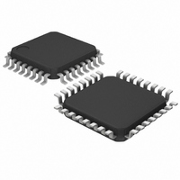
IC DVR CLK/DATA DUAL 1:5 32LQFP

MAX9312ECJ+

Manufacturer Part Number
MAX9312ECJ+
Description
IC DVR CLK/DATA DUAL 1:5 32LQFP
Manufacturer
Maxim Integrated Products
Type
Fanout Buffer (Distribution), Datar
Datasheet

Specifications of MAX9312ECJ+

Number Of Circuits
2
Ratio - Input:output
1:5
Differential - Input:output
Yes/Yes
Input
HSTL, LVECL, LVPECL
Output
LVECL, LVPECL
Frequency - Max
3GHz
Voltage - Supply
2.25 V ~ 3.8 V
Operating Temperature
-40°C ~ 85°C
Mounting Type
Surface Mount
Package / Case
32-LQFP
Frequency-max
3GHz
Lead Free Status / RoHS Status
Lead free / RoHS Compliant
The MAX9312/MAX9314 are low skew, dual 1-to-5 dif-
ferential drivers designed for clock and data distribu-
tion. These devices accept two inputs. Each input is
reproduced at five differential outputs. The differential
inputs can be adapted to accept single-ended inputs
by connecting the on-chip V
reference voltage.
The MAX9312/MAX9314 feature low part-to-part skew
(30ps) and output-to-output skew (12ps), making them
ideal for clock and data distribution across a backplane
or a board. For interfacing to differential HSTL and
LVPECL signals, these devices operate over a +2.25V
to +3.8V supply range, allowing high-performance clock
or data distribution in systems with a nominal +2.5V or
+3.3V supply. For differential LVECL operation, these
devices operate from a -2.25V to -3.8V supply.
The MAX9312 features an on-chip V
of 1.425V below the positive supply voltage. The
MAX9314 offers an on-chip V
1.32V below the positive supply voltage.
Both devices are offered in an industry-standard 32-pin
7mm x 7mm LQFP package. In addition, the MAX9312
is offered in a space-saving 32-pin 5mm x 5mm TQFN
package.
19-2079; Rev 2; 4/09
For pricing, delivery, and ordering information, please contact Maxim Direct at 1-888-629-4642,
or visit Maxim’s website at www.maxim-ic.com.
Pin Configuration appears at end of data sheet.
Precision Clock Distribution
Low-Jitter Data Repeater
CLKA
CLKA
75kΩ
V
BB
Dual 1:5 Differential LVPECL/LVECL/HSTL
________________________________________________________________ Maxim Integrated Products
V
75kΩ
EE
V
V
CC
EE
General Description
75kΩ
BB
supply to one input as a
BB
reference output of
Applications
BB
reference output
QA0
QA0
QA1
QA1
QA2
QA2
QA3
QA3
QA4
QA4
CLKB
CLKB
Clock and Data Drivers
75kΩ
o +2.25V to +3.8V Differential HSTL/LVPECL
o -2.25V to -3.8V Differential LVECL Operation
o 30ps (typ) Part-to-Part Skew
o 12ps (typ) Output-to-Output Skew
o 312ps (typ) Propagation Delay
o ≥ 300mV Differential Output at 3GHz
o On-Chip Reference for Single-Ended Inputs
o Output Low with Open Input
o Pin Compatible with MC100LVEP210 (MAX9312)
o Offered in Tiny QFN* Package (70% Smaller
* Exposed pad.
+ Denotes a lead(Pb)-free/RoHS-compliant package.
MAX9312ECJ+
MAX9312ETJ+
MAX9314ECJ
Operation
and MC100EP210 (MAX9314)
Footprint than LQFP)
75kΩ
V
EE
PART
V
V
CC
EE
75kΩ
-40°C to +85°C
-40°C to +85°C
-40°C to +85°C
TEMP RANGE
Ordering Information
Functional Diagram
QB0
QB0
QB1
QB1
QB2
QB2
QB3
QB3
QB4
QB4
PIN-PACKAGE
32 LQFP
32 TQFN-EP*
32 LQFP
Features
1

Related parts for MAX9312ECJ+

MAX9312ECJ+ Summary of contents

Page 1

... On-Chip Reference for Single-Ended Inputs o Output Low with Open Input o Pin Compatible with MC100LVEP210 (MAX9312) and MC100EP210 (MAX9314) o Offered in Tiny QFN* Package (70% Smaller reference output Footprint than LQFP) BB reference output of PART MAX9312ECJ+ MAX9312ETJ+ Applications MAX9314ECJ * Exposed pad. + Denotes a lead(Pb)-free/RoHS-compliant package. QA0 V CC QA0 QA1 75kΩ ...

Page 2

Dual 1:5 Differential LVPECL/LVECL/HSTL Clock and Data Drivers ABSOLUTE MAXIMUM RATINGS ...............................................................................4. Inputs (CLK_, CLK_) .............................V CLK_ to CLK_ ....................................................................±3.0V Continuous Output Current .................................................50mA Surge Output Current........................................................100mA V Sink/Source Current ...............................................±0.65mA BB Continuous Power Dissipation ...

Page 3

Dual 1:5 Differential LVPECL/LVECL/HSTL DC ELECTRICAL CHARACTERISTICS (continued +2.25V to +3.8V, outputs loaded with 50Ω ± PARAMETER SYMBOL CONDITIONS CLK_ Input Low I ILCLK Current OUTPUTS (Q__ Single-Ended Output ...

Page 4

Dual 1:5 Differential LVPECL/LVECL/HSTL Clock and Data Drivers AC ELECTRICAL CHARACTERISTICS ( +2.25V to +3.8V, outputs loaded with 50Ω ± (20% to 80%), 1. IHD EE CC ...

Page 5

Dual 1:5 Differential LVPECL/LVECL/HSTL (V = +3.3V 0.95V IHD CC loaded with 50Ω 2V +25°C, unless otherwise noted SUPPLY CURRENT vs. ...

Page 6

Dual 1:5 Differential LVPECL/LVECL/HSTL Clock and Data Drivers PIN NAME Positive Supply Voltage. Bypass from 16, 25 Place the capacitors as close to the device as possible with the smaller value capacitor closest to CC ...

Page 7

Dual 1:5 Differential LVPECL/LVECL/HSTL Detailed Description The MAX9312/MAX9314 are low-skew, dual 1-to-5 differ- ential drivers designed for clock and data distribution. For interfacing to differential HSTL and LVPECL signals, these devices operate over a +2.25V to +3.8V supply range, allowing ...

Page 8

Dual 1:5 Differential LVPECL/LVECL/HSTL Clock and Data Drivers CLK_ CLK_ Q_ Q_ Figure 1. Switching with Single-Ended Input CLK_ CLK_ Q_ Q_ (Q_) - (Q_) Figure 2. Differential Transition Time and Propagation Delay Timing Diagram Pin Configuration TOP VIEW V ...

Page 9

... Maxim cannot assume responsibility for use of any circuitry other than circuitry entirely embodied in a Maxim product. No circuit patent licenses are implied. Maxim reserves the right to change the circuitry and specifications without notice at any time. Maxim Integrated Products, 120 San Gabriel Drive, Sunnyvale, CA 94086 408-737-7600 _____________________ 9 © 2009 Maxim Integrated Products ...

Related keywords