NB7L111MMNG ON Semiconductor, NB7L111MMNG Datasheet - Page 5
NB7L111MMNG
Manufacturer Part Number
NB7L111MMNG
Description
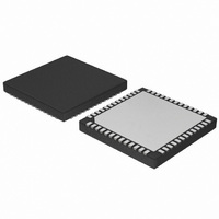
IC DRVR CLK/DATA 1:10 DIFF 52QFN
Manufacturer
ON Semiconductor
Type
Fanout Buffer (Distribution), Multiplexer , Datar
Datasheet
1.NB7L111MMNR2G.pdf
(13 pages)
Specifications of NB7L111MMNG
Number Of Circuits
1
Ratio - Input:output
2:10
Differential - Input:output
Yes/Yes
Input
CML, LVCMOS, LVDS, LVNECL, LVPECL, LVTTL
Output
CML
Frequency - Max
5.5GHz
Voltage - Supply
2.375 V ~ 3.465 V
Operating Temperature
-40°C ~ 85°C
Mounting Type
Surface Mount
Package / Case
52-VFQFN Exposed Pad
Frequency-max
5.5GHz
Output Logic Level
CML
Supply Voltage (max)
3.465 V
Supply Voltage (min)
2.375 V
Maximum Operating Temperature
+ 85 C
Maximum Data Rate
6 Gbps
Minimum Operating Temperature
- 40 C
Mounting Style
SMD/SMT
Number Of Clock Inputs
2
Supply Current
290 mA
Lead Free Status / RoHS Status
Lead free / RoHS Compliant
Available stocks
Company
Part Number
Manufacturer
Quantity
Price
Company:

Part Number:
NB7L111MMNG
Manufacturer:
ON Semiconductor
Quantity:
15
Part Number:
NB7L111MMNG
Manufacturer:
ON/安森美
Quantity:
20 000


NOTE: Device will meet the specifications after thermal equilibrium has been established when mounted in a test socket or printed circuit
6. CML outputs require 50 W receiver termination resistors to V
7. Input and output parameters vary 1:1 with V
8. V
9. V
Table 5. DC CHARACTERISTICS
DIFFERENTIAL INPUT DRIVEN SINGLE−ENDED (See Figures 13 and 15)
DIFFERENTIAL INPUTS DRIVEN DIFFERENTIALLY (See Figures 14 and 16)
Symbol
I
V
V
V
V
V
V
V
V
V
I
I
R
R
R
Coef
CC
IH
IL
OH
OL
th
IH
IL
IHD
ILD
CMR
ID
TIN
TOUT
Temp
th
CMR
is applied to the complementary input when operating in single−ended mode.
board with maintained transverse airflow greater than 500 lfpm. Electrical parameters are guaranteed only over the declared
operating temperature range. Functional operation of the device exceeding these conditions is not implied. Device specification limit
values are applied individually under normal operating conditions and not valid simultaneously.
(MIN) varies 1:1 with V
Power Supply Current (Inputs and Outputs Open)
Output HIGH Voltage (Notes 6 and 7)
Output LOW Voltage (Notes 6 and 7)
Input Threshold Reference Voltage Range (Note 8)
Single−ended Input HIGH Voltage (Note 7)
Single−ended Input LOW Voltage (Note 7)
Differential Input HIGH Voltage
Differential Input LOW Voltage
Input Common Mode Range (Differential Configuration) (Note 9)
Differential Input Voltage (V
Input HIGH Current
(Termination Pins Open)
Input LOW Current
(Termination Pins Open)
Internal Input Termination Resistor
Internal Output Termination Resistor
Internal I/O Termination Resistor Temperature Coefficient
EE
, V
CMR
IHD
V
(MAX) varies 1:1 with V
Characteristic
CC
− V
= 2.375 V 2.625 V and 3.135 V to 3.465 V, V
ILD
CC
)
.
V
V
V
V
http://onsemi.com
CC
CC
CC
CC
= 2.375 V to 2.625 V
= 3.135 V to 3.465 V
= 2.375 V to 2.625 V
= 3.135 V to 3.465 V
CC
CLK[0−1]/CLK[0−1]
CLK[0−1]/CLK[0−1]
CC
for proper operation.
.
5
SEL/SEL
SEL/SEL
EE
V
V
V
V
CC
CC
CC
1125
th
1200
1163
−100
−150
−100
−150
= 0 V, T
Min
V
V
255
270
75
45
45
− 440
− 490
EE
EE
+ 75
− 40
A
= −40°C to +85°C (Notes 6 and 7)
V
V
V
CC
CC
CC
−3.75
Typ
290
305
50
50
5
5
− 350
− 400
− 20
V
V
V
V
V
V
CC
CC
CC
CC
CC
CC
2500
Max
V
V
V
325
340
100
150
100
150
55
55
CC
CC
CC
– 290
− 340
– 150
– 75
– 75
– 37
mW/C
Unit
mA
mV
mV
mV
mV
mV
mV
mV
mV
mV
mA
mA
W
W
Related parts for NB7L111MMNG
Image
Part Number
Description
Manufacturer
Datasheet
Request
R

Part Number:
Description:
ON Semiconductor [VOLTAGE REGULATOR]
Manufacturer:
ON Semiconductor
Datasheet:
Part Number:
Description:
357-036-542-201 CARDEDGE 36POS DL .156 BLK LOPRO
Manufacturer:
ON Semiconductor
Datasheet:
Part Number:
Description:
357-036-542-201 CARDEDGE 36POS DL .156 BLK LOPRO
Manufacturer:
ON Semiconductor
Datasheet:
Part Number:
Description:
357-036-542-201 CARDEDGE 36POS DL .156 BLK LOPRO
Manufacturer:
ON Semiconductor
Datasheet:
Part Number:
Description:
357-036-542-201 CARDEDGE 36POS DL .156 BLK LOPRO
Manufacturer:
ON Semiconductor
Datasheet:
Part Number:
Description:
357-036-542-201 CARDEDGE 36POS DL .156 BLK LOPRO
Manufacturer:
ON Semiconductor
Datasheet:
Part Number:
Description:
357-036-542-201 CARDEDGE 36POS DL .156 BLK LOPRO
Manufacturer:
ON Semiconductor
Datasheet:
Part Number:
Description:
357-036-542-201 CARDEDGE 36POS DL .156 BLK LOPRO
Manufacturer:
ON Semiconductor
Datasheet:
Part Number:
Description:
357-036-542-201 CARDEDGE 36POS DL .156 BLK LOPRO
Manufacturer:
ON Semiconductor
Datasheet:
Part Number:
Description:
357-036-542-201 CARDEDGE 36POS DL .156 BLK LOPRO
Manufacturer:
ON Semiconductor
Datasheet:
Part Number:
Description:
357-036-542-201 CARDEDGE 36POS DL .156 BLK LOPRO
Manufacturer:
ON Semiconductor
Datasheet:
Part Number:
Description:
Manufacturer:
ON Semiconductor
Datasheet:
Part Number:
Description:
Manufacturer:
ON Semiconductor
Datasheet:
Part Number:
Description:
Manufacturer:
ON Semiconductor
Datasheet: