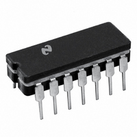
DS0026CJ National Semiconductor, DS0026CJ Datasheet

DS0026CJ
Specifications of DS0026CJ
Available stocks
Related parts for DS0026CJ
DS0026CJ Summary of contents
Page 1
... The DS0026 is designed to fulfill a wide variety of MOS inter- face requirements. Information on the correct usage of the DS0026 in these as well as other systems is included in the application note AN-76. Connection Diagram (Top View) © 2010 National Semiconductor Corporation 5853 Version 6 Revision 3 DS0026 Features ■ Fast rise and fall times—20 ns 1000 pF load ■ ...
Page 2
... Absolute Maximum Ratings If Military/Aerospace specified devices are required, please contact the National Semiconductor Sales Office/ Distributors for availability and specifications − (V − ) Differential Voltage Input Current Input Voltage (V ) − (V − Peak Output Current Ordering Information Order Number DS0026CN DS0026CMA DS0026CMM Electrical Characteristics ...
Page 3
Note 1: “Absolute Maximum Ratings” are those values beyond which the safety of the device cannot be guaranteed. Except for “Operating Temperature Range” they are not meant to imply that the devices should be operated at these limits. The table ...
Page 4
Rise Time vs Load Capacitance Recommended Input Coding Capacitance www.national.com 585325 585327 4 5853 Version 6 Revision 3 Print Date/Time: 2010/07/13 22:49:07 Fall Time vs Load Capacitance 585326 DC Power ( Duty Cycle 585328 ...
Page 5
Schematic Diagram AC Test Circuits and Switching Time Waveforms 5853 Version 6 Revision 3 1/2 DS0026 585312 FIGURE 1. 5 Print Date/Time: 2010/07/13 22:49:07 585310 585313 www.national.com ...
Page 6
Typical Applications AC Coupled MOS Clock Driver DC Coupled RAM Memory Address or Precharge Driver (Positive Supply Only) Application Hints DRIVING THE MM5262 WITH THE DS0026 CLOCK DRIVER The clock signals for the MM5262 have three requirements which have the ...
Page 7
Limiting the inductance of the clock lines can be accom- plished by minimizing their length and by laying out the lines such that the return current is closely coupled to the clock lines. When minimizing the length of clock lines ...
Page 8
Lastly, the clock lines must be considered as noise genera- tors. Figure 5 shows a clock coupled through a parasitic coupling capacitor eight data input lines being driven 7404. A parasitic lumped line inductance, ...
Page 9
Physical Dimensions inches (millimeters) unless otherwise noted 5853 Version 6 Revision 3 Molded Dual-In-Line Package (N) Order Number DS0026CN NS Package Number N08E 8-Lead Small Outline Molded package (M) NS Package Number M08A 9 Print Date/Time: 2010/07/13 22:49:07 www.national.com ...
Page 10
Mini SOIC Package (MM) NS Package Number MU08A 10 5853 Version 6 Revision 3 Print Date/Time: 2010/07/13 22:49:07 ...
Page 11
Notes 11 5853 Version 6 Revision 3 Print Date/Time: 2010/07/13 22:49:07 www.national.com ...
Page 12
... For more National Semiconductor product information and proven design tools, visit the following Web sites at: www.national.com Products Amplifiers www.national.com/amplifiers Audio www.national.com/audio Clock and Timing www.national.com/timing Data Converters www.national.com/adc Interface www.national.com/interface LVDS www.national.com/lvds Power Management www.national.com/power Switching Regulators www.national.com/switchers LDOs www.national.com/ldo LED Lighting www ...


