IDTCSP2510CPGG IDT, Integrated Device Technology Inc, IDTCSP2510CPGG Datasheet
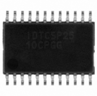
IC CLK DVR ZD BUFFER PLL 24TSSOP

IDTCSP2510CPGG

Manufacturer Part Number
IDTCSP2510CPGG
Description
IC CLK DVR ZD BUFFER PLL 24TSSOP
Manufacturer
IDT, Integrated Device Technology Inc
Type
PLL Driver, Zero Delay Bufferr
Datasheet

Specifications of IDTCSP2510CPGG

Pll
Yes with Bypass
Input
Clock
Output
Clock
Number Of Circuits
1
Ratio - Input:output
1:10
Differential - Input:output
No/No
Frequency - Max
140MHz
Divider/multiplier
No/No
Voltage - Supply
3 V ~ 3.6 V
Operating Temperature
0°C ~ 85°C
Mounting Type
Surface Mount
Package / Case
24-TSSOP
Frequency-max
140MHz
Lead Free Status / RoHS Status
Lead free / RoHS Compliant
Other names
800-1706
800-1706-5
800-1706
CSP2510CPGG

Available stocks

Company
Part Number
Manufacturer
Quantity
Price
Part Number:
IDTCSP2510CPGG
Manufacturer:
ATHEROS
Quantity:
6 770
Part Number:
IDTCSP2510CPGG
Manufacturer:
IDT
Quantity:
20 000
FEATURES:
• Phase-Lock Loop Clock Distribution for Synchronous DRAM
• Distributes one clock input to one bank of ten outputs
• Output enable bank control
• External feedback (FBIN) pin is used to synchronize the
• No external RC network required for PLL loop stability
• Operates at 3.3V V
• tpd Phase Error at 133MHz: < ±150ps
• Jitter (peak-to-peak) at 133MHz: < ±75ps @ 133MHz
• Spread Spectrum Compatible
• Operating frequency 25MHz to 140MHz
• Available in 24-Pin TSSOP package
APPLICATIONS:
• SDRAM Modules
• PC Motherboards
• Workstations
The IDT logo is a registered trademark of Integrated Device Technology, Inc.
0º º º º º C TO 85º º º º º C TEMPERATURE RANGE
IDTCSP2510C
3.3V PHASE-LOCK LOOP CLOCK DRIVER
c
Applications
outputs to the clock input signal
2008 Integrated Device Technology, Inc.
FUNCTIONAL BLOCK DIAGRAM
DD
AV
FBIN
CLK
DD
G
24
13
23
11
3.3V PHASE-LOCK LOOP
CLOCK DRIVER
ZERO DELAY BUFFER
PLL
1
DESCRIPTION:
loop (PLL) clock driver. It uses a PLL to precisely align, in both frequency
and phase, the feedback (FBOUT) output to the clock (CLK) input signal.
It is specifically designed for use with synchronous DRAMs. The CSP2510C
operates at 3.3V.
Output signal duty cycles are adjusted to 50 percent, independent of the
duty cycle at CLK. The outputs can be enabled or disabled via the control
G input. When the G input is high, the outputs switch in phase and frequency
with CLK; when the G input is low, the outputs are disabled to the logic-low
state.
external RC networks. The loop filter for the PLL is included on-chip,
minimizing component count, board space, and cost.
stabilization time to achieve phase lock of the feedback signal to the
reference signal. This stabilization time is required, following power up and
application of a fixed-frequency, fixed-phase signal at CLK, as well as
following any changes to the PLL reference or feedback signals. The PLL
can be bypassed for the test purposes by strapping AV
device is also available (on special order) in Industrial temperature range
(-40°C to +85°C). See ordering information for details.
The CSP2510C is a high performance, low-skew, low-jitter, phase-lock
One bank of ten outputs provide low-skew, low-jitter copies of CLK.
Unlike many products containing PLLs, the CSP2510C does not require
Because it is based on PLL circuitry, the CSP2510C requires a
The CSP2510C is specified for operation from 0°C to +85°C. This
12
16
17
20
21
15
3
4
5
8
9
Y0
Y1
Y2
Y3
Y4
FBOUT
Y5
Y6
Y7
Y8
Y9
0ºC TO 85ºC TEMPERATURE RANGE
NOVEMBER 2008
IDTCSP2510C
DD
to ground.
DSC-5180/4

Related parts for IDTCSP2510CPGG

IDTCSP2510CPGG Summary of contents

Page 1

IDTCSP2510C 3.3V PHASE-LOCK LOOP CLOCK DRIVER FEATURES: • Phase-Lock Loop Clock Distribution for Synchronous DRAM Applications • Distributes one clock input to one bank of ten outputs • Output enable bank control • External feedback (FBIN) pin is used to ...

Page 2

IDTCSP2510C 3.3V PHASE-LOCK LOOP CLOCK DRIVER PIN CONFIGURATION AGND GND 7 GND FBOUT 12 TSSOP TOP VIEW RECOMMENDED OPERATING CONDITIONS ...

Page 3

IDTCSP2510C 3.3V PHASE-LOCK LOOP CLOCK DRIVER PIN DESCRIPTION Terminal Name No. Type CLK 24 I Clock input. CLK provides the clock signal to be distributed by the CSP2510C clock driver. CLK is used to provide the reference signal to the ...

Page 4

IDTCSP2510C 3.3V PHASE-LOCK LOOP CLOCK DRIVER DC ELECTRICAL CHARACTERISTICS OVER OPERATING FREE-AIR TEMPERA- TURE RANGE (1) Symbol Description V Input Clamp Voltage IK V Input HIGH Level IH V Input LOW Level IL V HIGH Level Output Voltage OH V ...

Page 5

IDTCSP2510C 3.3V PHASE-LOCK LOOP CLOCK DRIVER SWITCHING CHARACTERISTICS OVER OPERATING RANGE OF SUPPLY VOLTAGE AND OPERATING FREE-AIR TEMPERATURE, C Parameter (2) From (Input) t error 100MHz < CLK↑ < 133MHz PHASE (3) t error – jitter CLK↑ = 133MHz PHASE ...

Page 6

IDTCSP2510C 3.3V PHASE-LOCK LOOP CLOCK DRIVER PARAMETER MEASUREMENT INFORMATION From Output Under Test C =30pF L Y CLK CSP2510C F BOUT F BIN C F PCB TRACE NOTES: 1. All inputs pulses are supplied by generators having ...

Page 7

IDTCSP2510C 3.3V PHASE-LOCK LOOP CLOCK DRIVER TYPICAL CHARACTERISTICS 200 150 100 -50 -100 -150 -200 Phase Error vs Clock Frequency AV and ...

Page 8

IDTCSP2510C 3.3V PHASE-LOCK LOOP CLOCK DRIVER TYPICAL CHARACTERISTICS (CONT 100 Output Duty Cycle vs Clock Frequency AV and V = 3.3V DD ...

Page 9

IDTCSP2510C 3.3V PHASE-LOCK LOOP CLOCK DRIVER ORDERING INFORMATION CSP XXXXX XX Device Type Package CORPORATE HEADQUARTERS 6024 Silver Creek Valley Road San Jose, CA 95138 X Process Blank 0°C to +85°C (standard) I -40°C to +85°C (Industrial) PG Thin Shrink ...

Related keywords