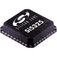
SI5325C-C-GM Silicon Laboratories Inc, SI5325C-C-GM Datasheet - Page 10

SI5325C-C-GM
Manufacturer Part Number
SI5325C-C-GM
Description
IC UP-PROG CLK MULTIPLIER 36-QFN
Manufacturer
Silicon Laboratories Inc
Type
Clock Multiplierr
Datasheet
1.SI5325C-C-GM.pdf
(52 pages)
Specifications of SI5325C-C-GM
Number Of Circuits
1
Package / Case
36-QFN
Pll
Yes
Input
Clock
Output
CML, CMOS, LVDS, LVPECL
Ratio - Input:output
2:2
Differential - Input:output
Yes/Yes
Frequency - Max
346MHz
Divider/multiplier
Yes/Yes
Voltage - Supply
1.71 V ~ 3.63 V
Operating Temperature
-40°C ~ 85°C
Mounting Type
Surface Mount
Frequency-max
346MHz
Maximum Input Frequency
710 MHz
Minimum Input Frequency
10 MHz
Output Frequency Range
10 MHz to 346 MHz
Supply Voltage (max)
3.63 V
Supply Voltage (min)
1.71 V
Maximum Operating Temperature
+ 85 C
Minimum Operating Temperature
- 40 C
Mounting Style
SMD/SMT
Operating Supply Voltage
1.8 V, 2.5 V, 3.3 V
Lead Free Status / RoHS Status
Lead free / RoHS Compliant
Available stocks
Company
Part Number
Manufacturer
Quantity
Price
Part Number:
SI5325C-C-GM
Manufacturer:
SILICONLABS/èٹ¯ç§‘
Quantity:
20 000
Si5325
10
Note: Internal register names are indicated by underlined italics, e.g., INT_PIN. See Si5325 Register Map.
5, 10, 11,
6, 8, 19,
15, 32
20 31
Pin #
12
13
16
17
21
4
Pin Name
CKIN2+
CKIN1+
CKIN2–
CKIN1–
CS_CA
GND
C2B
V
DD
Table 3. Si5325 Pin Descriptions (Continued)
GND
V
I/O
I/O
O
DD
I
I
Signal Level
LVCMOS
LVCMOS
Supply
Supply
Multi
Multi
Preliminary Rev. 0.4
CKIN2 Invalid Indicator.
This pin functions as a LOS (and optionally FOS) alarm indi-
cator for CKIN2 if CK2_BAD_PIN = 1.
0 = CKIN2 present.
1 = LOS (FOS) on CKIN2.
The active polarity can be changed by CK_BAD_POL. If
CK2_BAD_PIN = 0, the pin tristates.
Supply.
The device operates from a 1.8, 2.5, or 3.3 V supply. Bypass
capacitors should be associated with the following VDD pins:
5
10
32
A 1.0 µF should also be placed as close to device as is prac-
tical.
Ground.
Must be connected to system ground. Minimize the ground
path impedance for optimal performance of this device.
Clock Input 2.
Differential input clock. This input can also be driven with a
single-ended signal. Input frequency range is 10 to 710 MHz.
Clock Input 1.
Differential input clock. This input can also be driven with a
single-ended signal. Input frequency range is 10 to 710 MHz.
Input Clock Select/Active Clock Indicator.
Input: In manual clock selection mode, this pin functions as
Output: In automatic clock selection mode, this pin indicates
the manual input clock selector if the CKSEL_PIN is
set to 1.
0 = Select CKIN1.
1 = Select CKIN2.
If CKSEL_PIN = 0, the CKSEL_REG register bit
controls this function. If configured as input, must be
set high or low.
which of the two input clocks is currently the active
clock. If alarms exist on both clocks, CA will indicate
the last active clock that was used before entering
the VCO freeze state. The CK_ACTV_PIN register
bit must be set to 1 to reflect the active clock status
to the CA output pin.
0 = CKIN1 active input clock.
1 = CKIN2 active input clock.
If CK_ACTV_PIN = 0, this pin will tristate. The CA
status will always be reflected in the
CK_ACTV_REG read only register bit.
0.1 µF
0.1 µF
0.1 µF
Description


