SY100S838ZC Micrel Inc, SY100S838ZC Datasheet

IC CLOCK GEN 3.3V/5V 20-SOIC

SY100S838ZC

Manufacturer Part Number
SY100S838ZC
Description
IC CLOCK GEN 3.3V/5V 20-SOIC
Manufacturer
Micrel Inc
Series
Precision Edge®r
Type
Clock Generatorr
Datasheet

Specifications of SY100S838ZC

Pll
No
Input
ECL, PECL
Output
Clock
Number Of Circuits
1
Ratio - Input:output
1:4
Differential - Input:output
Yes/Yes
Frequency - Max
1GHz
Divider/multiplier
Yes/No
Voltage - Supply
4.2 V ~ 5.5 V
Operating Temperature
0°C ~ 85°C
Mounting Type
Surface Mount
Package / Case
20-SOIC (7.5mm Width)
Frequency-max
1GHz
Lead Free Status / RoHS Status
Contains lead / RoHS non-compliant

Available stocks

Company
Part Number
Manufacturer
Quantity
Price
Part Number:
SY100S838ZC
Manufacturer:
SYNERGY
Quantity:
146
Part Number:
SY100S838ZC
Manufacturer:
SYNERGY
Quantity:
20 000
NOTES:
Z = LOW-to-HIGH transition
ZZ = HIGH-to-LOW transition
Micrel, Inc.
■ 3.3V and 5V power supply options
■ 50ps output-to-output skew
■ Synchronous enable/disable
■ Master Reset for synchronization
■ Internal 75K
■ Available in 20-pin SOIC package
Precision Edge is a registered trademark of Micrel, Inc.
M9999-113006
hbwhelp@micrel.com or (408) 955-1690
F
PIN NAMES
FEATURES
TRUTH TABLE
SEL
H
H
L
L
CLK
ZZ
X
Z
CLK
F
EN
MR
V
Q
Q
DIVSEL
SEL
BB
0,
2,
Pin
DIVSEL
Q
Q
1
3
H
H
L
L
input pull-down resistors
EN
H
X
L
Q
0,
Divide by 2
Divide by 2
Divide by 1
Divide by 1
Differential Clock Inputs
Function Select Input
Synchronous Enable
Master Reset
Reference Output
Differential ÷1 or ÷2 Outputs
Differential ÷2/3 or ÷4/6 Outputs
Frequency Select Input
Q
1
OUTPUTS
MR
H
L
L
Function
Q
Divide
Hold Q
Reset Q
2,
Divide by 4
Divide by 6
Divide by 2
Divide by 3
Q
Function
3
(
CLOCK GENERATION CHIP
OUTPUTS
÷
0–3
0–3
1,
÷
2/3) OR (
1
6) clock generation chip designed explicitly for low skew
clock generation applications. The internal dividers are
synchronous to each other, therefore, the common output
edges are all precisely aligned. The devices can be driven
by either a differential or single-ended ECL or, if positive
power supplies are used, PECL input signal. In addition,
by using the V
coupled into the device. If a single-ended input is to be
used, the V
input and bypassed to ground via a 0.01µF capacitor.
The V
reference for the input of the SY100S838/L under single-
ended input conditions. As a result, this pin can only
source/sink up to 0.5mA of current.
what clock generation chip function is. When FS
is LOW, SY100S838/L functions as a divide by 2 and by
4/6 clock generation chip. However, if FS
it functions as a divide by 1 and by 2/3 clock chip.
internal dividers will only be enabled/disabled when the
internal clock is already in the LOW state. This avoids
any chance of generating a runt clock pulse on the
internal clock when the device is enabled/disabled as
can happen with an asynchronous control. An internal
runt pulse could lead to losing synchronization between
the internal divider stages. The internal enable flip-flop is
clocked on the falling edge of the input clock, therefore,
all associated specification limits are referenced to the
negative edge of the clock input.
state; the master reset (MR) input allows for the
synchronization of the internal dividers, as well as for
multiple SY100S838/Ls in a system.
DESCRIPTION
The SY100S838/L is a low skew (÷1, ÷2/3) or (÷2, ÷4/
The Function Select (F
The common enable (EN) is synchronous so that the
Upon start-up, the internal flip-flops will attain a random
÷
BB
2,
÷
output is designed to act as the switching
4/6)
BB
BB
output should be connected to the CLK
output, a sinusoidal source can be AC-
SEL
) input is used to determine
Precision Edge
Rev.: G
Issue Date: November 2006
SY100S838L
Precision Edge
EL
SY100S838
Precision Edge
input is HIGH,
SY100S838L
SY100S838
Amendment: /0
EL
input
®
®
®

Related parts for SY100S838ZC

SY100S838ZC Summary of contents

Page 1

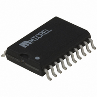
Micrel, Inc. FEATURES ■ 3.3V and 5V power supply options ■ 50ps output-to-output skew ■ Synchronous enable/disable ■ Master Reset for synchronization ■ Internal 75K Ω input pull-down resistors ■ Available in 20-pin SOIC package TRUTH TABLE CLK EN MR ...

Page 2

... SY100S838LZGTR Z20-1 Notes: 1. Tape and Reel. 2. Pb-Free package is recommended for new designs. 2 Precision Edge SY100S838L Operating Package Range Marking Commercial SY100S838ZC Commercial SY100S838ZC Commercial SY100S838LZC Commercial SY100S838LZC Industrial SY100S838ZI Industrial SY100S838ZI Industrial SY100S838LZI Industrial SY100S838LZI Industrial SY100S838ZG with Pb-Free bar-line indicator Pb-Free ...

Page 3

Micrel, Inc. BLOCK DIAGRAM CLK CLK SEL DIVSEL DC ELECTRICAL CHARACTERISTICS (Min (Max.); Symbol Parameter I Power Supply Current EE V Output Reference Voltage BB I Input ...

Page 4

Micrel, Inc. AC ELECTRICAL CHARACTERISTICS (Min (Max.); Symbol Parameter f Maximum Toggle Frequency MAX t Propagation Delay to Output PLH ➝ t CLK Output (Diff.) PHL ➝ CLK Output (S.E.) ...

Page 5

Micrel, Inc. 20-PIN SOIC .300" WIDE (Z20-1) MICREL, INC. 2180 FORTUNE DRIVE SAN JOSE, CA 95131 USA + 1 (408) 944-0800 TEL The information furnished by Micrel in this datasheet is believed to be accurate and reliable. However, no responsibility ...

Related keywords