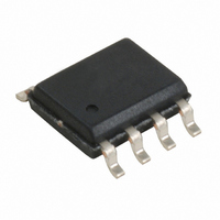
CY241V8ASXC-12 Cypress Semiconductor Corp, CY241V8ASXC-12 Datasheet - Page 4

CY241V8ASXC-12
Manufacturer Part Number
CY241V8ASXC-12
Description
IC CLOCK GEN MPEG W/VCXO 8SOIC
Manufacturer
Cypress Semiconductor Corp
Type
Clock Generator, Fanout Distributionr
Datasheet
1.CY241V8ASXC-12.pdf
(6 pages)
Specifications of CY241V8ASXC-12
Number Of Circuits
1
Package / Case
8-SOIC (3.9mm Width)
Pll
Yes with Bypass
Input
Clock
Output
Clock
Ratio - Input:output
1:2
Differential - Input:output
No/No
Frequency - Max
74.25MHz
Divider/multiplier
Yes/No
Voltage - Supply
3.135 V ~ 3.465 V
Operating Temperature
0°C ~ 70°C
Mounting Type
Surface Mount
Frequency-max
74MHz
Minimum Input Frequency
27 MHz
Output Frequency Range
74.25 MHz
Supply Voltage (max)
3.465 V
Supply Voltage (min)
3.135 V
Maximum Operating Temperature
+ 70 C
Minimum Operating Temperature
0 C
Mounting Style
SMD/SMT
Operating Supply Voltage
3.3 V
Lead Free Status / RoHS Status
Lead free / RoHS Compliant
Document #: 38-07676 Rev. **
AC Electrical Specifications
Test and Measurement Set-up
Voltage and Timing Definitions
Ordering Information
t
t
t
t
t
CY241V8ASXC-12
CY241V8ASXC-12T
Parameter
9
9
9
9
10
Ordering Code
[3]
Clock Jitter 74.25 MHz
Clock Jitter XBUF/27 MHz
Clock Jitter 74.25 MHz
Clock Jitter XBUF/27 MHz
PLL Lock Time
Package
Name
SZ08
SZ08
Name
Clock
Output
Clock
Output
VDD
8-pin SOIC – Tape and Reel Commercial
8-pin SOIC
(V
0.1 µF
Figure 2. ER = (0.6 x V
DD
t
= 3.3V) (continued)
3
Package Type
Figure 1. Duty Cycle Definition
Peak-to-peak period jitter
Peak-to-peak period jitter
1000-cycle long term jitter
1000-cycle long term jitter
t
2
GND
t
1
DUT
DD
[3]
) /t3, EF = (0.6 x V
Description
Commercial
Operating Range
t
4
V
80% of V
20% of V
0V
DD
V
50% of V
0V
C
DD
DD
LOAD
Outputs
) /t4
3.3V
3.3V
Operating
Voltage
DD
DD
DD
Min.
–
–
–
–
–
Linear VCXO control curve
Linear VCXO control curve
CY241V08A-12
Typ.
150
250
430
270
–
Features
Max.
–
–
–
–
3
Page 4 of 6
Unit
ms
ps
ps
ps
ps
[+] Feedback


