NB2870ASNR2 ON Semiconductor, NB2870ASNR2 Datasheet
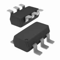
IC CLOCK SYNTHESIZR 4MA TSOT-6

NB2870ASNR2

Manufacturer Part Number
NB2870ASNR2
Description
IC CLOCK SYNTHESIZR 4MA TSOT-6
Manufacturer
ON Semiconductor
Type
Clock/Frequency Synthesizerr
Datasheet

Specifications of NB2870ASNR2

Pll
Yes
Input
CMOS, Crystal
Output
CMOS
Number Of Circuits
1
Ratio - Input:output
1:2
Differential - Input:output
No/No
Frequency - Max
30MHz
Divider/multiplier
Yes/No
Voltage - Supply
2.375 V ~ 3.6 V
Operating Temperature
0°C ~ 70°C
Mounting Type
Surface Mount
Package / Case
SC-74-6
Frequency-max
30MHz
Function
Clock Synthesizer
Operating Temperature (max)
70C
Operating Temperature (min)
0C
Pin Count
6
Mounting
Surface Mount
Lead Free Status / RoHS Status
Contains lead / RoHS non-compliant

Available stocks

Company
Part Number
Manufacturer
Quantity
Price
Part Number:
NB2870ASNR2
Manufacturer:
ON
Quantity:
2 500
Part Number:
NB2870ASNR2G
Manufacturer:
FAI
Quantity:
4 820
NB2870A
Low Power, Reduced EMI
Clock Synthesizer
designed specifically for a wide range of clock frequencies. The
NB2870A reduces ElectroMagnetic Interference (EMI) at the clock
source, allowing system wide reduction of EMI of all clock dependent
signals. The NB2870A allows significant system cost savings by
reducing the number of circuit board layers, ferrite beads and
shielding that are traditionally required to pass EMI regulations.
profile approved by the FCC and is implemented by using a
proprietary all digital method.
“spread” the bandwidth of a synthesized clock, and more importantly,
decreases the peak amplitudes of its harmonics. This results in
significantly lower system EMI compared to the typical narrow band
signal produced by oscillators and most frequency generators.
Lowering EMI by increasing a signal’s bandwidth is called ‘spread
spectrum clock generation’.
low power requirements like MP3 players, Notebooks and digital still
cameras.
Features
 Semiconductor Components Industries, LLC, 2010
November, 2010 - - Rev. 4
The NB2870A is a versatile spread spectrum frequency modulator
The NB2870A uses the most efficient and optimized modulation
The NB2870A modulates the output of a single PLL in order to
The NB2870A is targeted towards all portable devices with very
Frequency
Generates an EMI Optimized Clocking Signal at the Output
Integrated Loop Filter Components
Operates with a 3.3 V / 2.5 V Supply
Operating Current less than 4.0 mA
Low Power CMOS Design
Input Frequency Range: 13 MHz to 30 MHz
Generates a 1X Low EMI Spread Spectrum clock of the Input
Frequency Deviation 0.75% (TYP) @ 22 MHz
Available in TSOP- -6 Package (TSOT- -23- -6)
Pb- -Free Package is Available
1
See detailed ordering and shipping information in the package
dimensions section on page 7 of this data sheet.
6
*For additional marking information, refer to
(Note: Microdot may be in either location)
Application Note AND8002/D.
1
ORDERING INFORMATION
E09 = Specific Device Code
A
Y
W
G
http://onsemi.com
(TSOT- -23- -6)
= Assembly Location
= Year
= Work Week
= Pb--Free Package
CASE 318G
SN SUFFIX
TSOP- -6
Publication Order Number:
1
DIAGRAM*
MARKING
XXXAYWG
NB2870A/D
G

Related parts for NB2870ASNR2

NB2870ASNR2 Summary of contents

Page 1

NB2870A Low Power, Reduced EMI Clock Synthesizer The NB2870A is a versatile spread spectrum frequency modulator designed specifically for a wide range of clock frequencies. The NB2870A reduces ElectroMagnetic Interference (EMI) at the clock source, allowing system wide reduction of ...

Page 2

XIN/CLKIN Crystal Frequency XOUT Oscillator Feedback REFOUT Table 1. KEY SPECIFICATIONS Description Supply Voltages Frequency Range Cycle--to--Cycle Jitter Output Duty Cycle Modulation Equation Frequency Deviation REFOUT XIN/CLKIN Table 2. PIN DESCRIPTION Pin # Pin Name Type 1 REFOUT O Buffered ...

Page 3

Table 3. MAXIMUM RATINGS Symbol V V Voltage on any pin with respect to Ground DD Storage Temperature STG T Operating Temperature A T Max. Soldering Temperature (10 sec Junction Temperature J T Static Discharge Voltage ...

Page 4

Table 4. DC ELECTRICAL CHARACTERISTICS FOR 2.5 V SUPPLY temperature 25C) Symbol V Input LOW Voltage IL V Input HIGH Voltage IH I Input LOW Current IL I Input HIGH Current IH I XOUT Output LOW Current (@ 0.5 V, ...

Page 5

Table 6. DC ELECTRICAL CHARACTERISTICS FOR 3.3 V SUPPLY temperature 25C) Symbol V Input LOW Voltage IL V Input HIGH Voltage IH I Input LOW Current IL I Input HIGH Current IH I XOUT Output LOW Current (@ 0.4 V, ...

Page 6

Table 8. TYPICAL CRYSTAL SPECIFICATIONS Nominal Frequency Frequency Tolerance Operating Temperature Range Storage Temperature Load Capacitance Shunt Capacitance ESR XIN XOUT R1 = 510 Ω Crystal Figure 4. Typical Crystal Oscillator Circuit ...

Page 7

... ORDERING INFORMATION Device Marking NB2870ASNR2 E09 NB2870ASNR2G E09 †For information on tape and reel specifications, including part orientation and tape sizes, please refer to our Tape and Reel Packaging Specifications Brochure, BRD8011/D. Temperature Range Package 0C -- 70C TSOP--6 (TSOT--23--6) 0C -- 70C TSOP--6 ...

Page 8

... A 0.05 A1 *For additional information on our Pb--Free strategy and soldering details, please download the ON Semiconductor Soldering and Mounting Techniques Reference Manual, SOLDERRM/D. ON Semiconductor and are registered trademarks of Semiconductor Components Industries, LLC (SCILLC). SCILLC reserves the right to make changes without further notice to any products herein. SCILLC makes no warranty, representation or guarantee regarding the suitability of its products for any particular purpose, nor does SCILLC assume any liability arising out of the application or use of any product or circuit, and specifically disclaims any and all liability, including without limitation special, consequential or incidental damages. “ ...

Related keywords