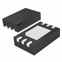
LTC6990CDCB#TRMPBF Linear Technology, LTC6990CDCB#TRMPBF Datasheet - Page 8

LTC6990CDCB#TRMPBF
Manufacturer Part Number
LTC6990CDCB#TRMPBF
Description
IC MPU SUPERVISORY 6DFN
Manufacturer
Linear Technology
Datasheet
1.LTC6990CDCBTRMPBF.pdf
(28 pages)
Specifications of LTC6990CDCB#TRMPBF
Frequency
*
Voltage - Supply
*
Current - Supply
235µA
Operating Temperature
*
Package / Case
6-WFDFN Exposed Pad
Count
*
Lead Free Status / RoHS Status
Lead free / RoHS Compliant
Other names
LTC6990CDCB#TRMPBFTR
Available stocks
Company
Part Number
Manufacturer
Quantity
Price
PIN FUNCTIONS
LTC6990
V
ply must be kept free from noise and ripple. It should be
bypassed directly to the GND pin with a 0.1μF capacitor.
DIV (Pin 2/Pin 4): Programmable Divider and Hi-Z Mode
Input. A V
pin voltage (V
V
and GND. Use 1% resistors to ensure an accurate result.
The DIV pin and resistors should be shielded from the
OUT pin or any other traces that have fast edges. Limit
the capacitance on the DIV pin to less than 100pF so that
V
mines the behavior of the output when OE is driven low.
If Hi-Z = 0 the output is pulled low when disabled. If Hi-Z
= 1 the output is placed in a high impedance condition
when disabled.
SET (Pin 3/Pin 3): Frequency-Setting Input. The voltage
on the SET pin (V
amount of current sourced from the SET pin (I
grams the master oscillator frequency. The I
range is 1.25μA to 40μA. The output oscillation will stop
if I
nected between SET and GND is the most accurate way to
set the frequency. For best performance, use a precision
metal or thin fi lm resistor of 0.5% or better tolerance and
50ppm/°C or better temperature coeffi cient. For lower ac-
curacy applications an inexpensive 1% thick fi lm resistor
may be used.
8
+
DIV
DIV
SET
(Pin 1/Pin 5): Supply Voltage (2.25V to 5.5V). This sup-
may be generated by a resistor divider between V
settles quickly. The MSB of DIVCODE (Hi-Z) deter-
drops below approximately 500nA. A resistor con-
+
referenced A/D converter monitors the DIV
DIV
) to determine a 4-bit result (DIVCODE).
SET
) is regulated to 1V above GND. The
(DCB/S6)
SET
SET
current
) pro-
+
Limit the capacitance on the SET pin to less than 10pF
to minimize jitter and ensure stability. Capacitance less
than 100pF maintains the stability of the feedback circuit
regulating the V
OE (Pin 4/Pin 1): Output Enable. Drive high to enable the
output driver (Pin 6). Driving OE low disables the output
asynchronously, so that the output is immediately forced
low (Hi-Z = 0) or fl oated (Hi-Z = 1). When enabled, the
output may temporarily remain low to synchronize with
the internal oscillator in order to eliminate pulse slivers.
GND (Pin 5/Pin 2): Ground. Tie to a low inductance ground
plane for best performance.
OUT (Pin 6/Pin 6): Oscillator Output. The OUT pin swings
from GND to V
30Ω. When driving an LED or other low-impedance load a
series output resistor should be used to limit source/sink
current to 20mA.
+
with an output resistance of approximately
SET
V
+
R
voltage.
SET
OE
GND
SET
LTC6990
OUT
6990 PF
DIV
V
+
C1
0.1μF
V
+
R1
R2
6990f


