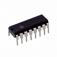
TC500CPE Microchip Technology, TC500CPE Datasheet - Page 14

TC500CPE
Manufacturer Part Number
TC500CPE
Description
IC ANALOG FRONT END 16BIT 16DIP
Manufacturer
Microchip Technology
Specifications of TC500CPE
Number Of Bits
16
Number Of Channels
1
Power (watts)
10mW
Voltage - Supply, Analog
5V
Voltage - Supply, Digital
4.5 V ~ 7.5 V
Package / Case
16-DIP (0.300", 7.62mm)
Resolution (bits)
17bit
Sampling Rate
10SPS
Input Channel Type
Differential
Data Interface
3-Wire, Serial
Supply Voltage Range - Analog
± 4.5V To ± 7.5V
Supply Current
1mA
Lead Free Status / RoHS Status
Lead free / RoHS Compliant
Other names
158-1021
158-1021
158-1021
Available stocks
Company
Part Number
Manufacturer
Quantity
Price
TC500/A/510/514
FIGURE 8-1:
8.6
The comparator delay and the controller's response
latency may result in overshoot, causing charge
buildup on the integrator at the end of a conversion.
This charge must be removed or performance will
degrade. The integrator output zero phase should be
activated (AB = 00) until CMPTR goes high. It is
absolutely critical that this phase be terminated
immediately so that overshoot is not allowed to occur in
the opposite direction. At this point, it can be assured
that the integrator is near zero. Auto-zero should be
entered (AB = 01) and the TC5XX held in this state until
the next cycle is begun (see Figure 8-2).
FIGURE 8-2:
DS21428C-page 14
Comparator
Output Comp
Integrator
Output
N
TH
S
Integrate
Integrator Output Zero Phase
Phase
Low V
REF
Noise Threshold.
Overshoot.
De-integrate Phase
Overshoot
30V
Crossing
Zero
Slope (S) =
Zero Phase
Integrator
N
TH
R
S
INT
V
REF
Normal V
C
INT
8.7
8.7.1
A capacitive charge pump is employed to invert the
voltage on V
TC514. This voltage is also available on the V
to provide negative bias elsewhere in the system. Two
external capacitors are required to perform the
conversion.
Timing is generated by an internal state machine driven
from an on-board oscillator. During the first phase,
capacitor C
charged to V
C
runs at 100 kHz to ensure minimum output ripple. This
frequency can be reduced by placing a capacitor from
OSC to V
value is shown in Section 2.0 “Typical Performance
Curves”.
8.7.2
The TC514 is equipped with a four-input differential
analog multiplexer. Input channels are selected using
select inputs (A1, A0). These are high-true control
signals (i.e., channel 0 is selected when (A1, A0 = 00).
N
OUT
TH
REF
- during the second phase. The oscillator normally
= Noise Threshold
Using the TC510/TC514
DD
F
NEGATIVE SUPPLY VOLTAGE
CONVERTER (TC510, TC514)
ANALOG INPUT MULTIPLEXER
(TC514)
S
. The relationship between the capacitor
is switched across the power supply and
DD
+. This charge is transferred to capacitor
for negative bias within the TC510/
2004 Microchip Technology Inc.
N
TH
High V
S
REF
OUT
- pin


