TC500CPE Microchip Technology, TC500CPE Datasheet - Page 3
TC500CPE
Manufacturer Part Number
TC500CPE
Description
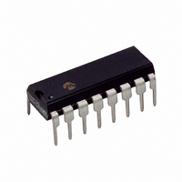
IC ANALOG FRONT END 16BIT 16DIP
Manufacturer
Microchip Technology
Specifications of TC500CPE
Number Of Bits
16
Number Of Channels
1
Power (watts)
10mW
Voltage - Supply, Analog
5V
Voltage - Supply, Digital
4.5 V ~ 7.5 V
Package / Case
16-DIP (0.300", 7.62mm)
Resolution (bits)
17bit
Sampling Rate
10SPS
Input Channel Type
Differential
Data Interface
3-Wire, Serial
Supply Voltage Range - Analog
± 4.5V To ± 7.5V
Supply Current
1mA
Lead Free Status / RoHS Status
Lead free / RoHS Compliant
Other names
158-1021
158-1021
158-1021
Available stocks
Company
Part Number
Manufacturer
Quantity
Price


1.0
Absolute Maximum Ratings†
TC510/TC514 Positive Supply Voltage
TC500/TC500A Supply Voltage
TC500/TC500A Positive Supply Voltage
TC500/TC500A Negative Supply Voltage
Analog Input Voltage (V
Logic Input Voltage...............V
Voltage on OSC:
Ambient Operating Temperature Range:
Storage Temperature Range: ............. -65°C to +150°C
DC CHARACTERISTICS
© 2008 Microchip Technology Inc.
........................... -0.3V to (V
................................................................ 0°C to +70°C
Electrical Specifications: Unless otherwise specified, TC510/TC514: V
C
Analog
Resolution
Zero-scale Error with
Auto-zero Phase
End Point Linearity
Best-Case Straight
Line Linearity
Zero-scale Temp.
Coefficient
Full-scale Symmetry
Error (Rollover Error)
Full-scale
Temperature
Coefficient
Input Current
Common Mode
Voltage Range
Integrator Output
Swing
Analog Input Signal
Range
Note 1:
AZ
= C
Parameters
(V
(V
(V
(V
2:
3:
REF
ELECTRICAL
CHARACTERISTICS
DD
DD
DD
SS
Integrate time ≥ 66 ms, auto-zero time ≥ 66 ms, V
End point linearity at ±1/4, ±1/2, ±3/4 F.S. after full-scale adjustment.
Rollover error is related to C
= 0.47
to V
to GND)................................................-8V
to GND) ......................................... +10.5V
to GND) ............................................ +12V
SS
μ
) .............................................. +18V
F.
V
ZS
FS
Sym
ZSE
ENL
SYE
IN
NL
I
CMR
IN
+ or V
TC
TC
DD
DD
V
V
V
IN
SS
SS
SS
+0.3V) for V
Min.
-) ............V
+0.3V to GND - 0.3V
60
—
—
—
—
—
—
—
—
—
—
+ 1.5
+ 0.9
+ 1.5
INT
T
, C
A
0.005
0.003
= +25°C
REF
Typ.
0.01
—
—
—
—
—
—
—
—
—
—
6
DD
DD
, C
AZ
< 5.5V
to V
V
V
V
DD
DD
DD
characteristics.
0.005
0.003
0.015
0.010
0.008
0.005
Max.
SS
—
—
—
—
—
– 1.5 V
– 0.9 V
– 1.5 V
INT
(peak) ≈ 4V.
SS
SS
SS
Min.
—
—
—
—
—
—
—
—
—
—
—
† Notice: Stresses above those listed under “Absolute
Maximum Ratings” may cause permanent damage to
the device. These are stress ratings only and functional
operation of the device at these or any other conditions
above those indicated in the operation sections of the
specifications is not implied. Exposure to Absolute
Maximum Rating conditions for extended periods may
affect device reliability.
+ 1.5
+ 0.9
+ 1.5
T
DD
A
= 0°C to 70°C
= +5V, TC500/TC500A: V
0.005
0.015
0.010
0.003
Typ.
0.03
10
—
—
—
—
—
—
—
1
TC500/A/510/514
V
V
V
SS
DD
SS
0.012
0.009
0.060
0.045
Max.
—
—
—
—
—
—
2
+ 0.9
– 1.5
+ 1.5
ppm/°C Over Operating
% F.S.
% F.S.
% F.S.
% F.S. TC500/TC510/TC514
% F.S. TC500/TC510/TC514,
% F.S. TC500A
μ
Units
V/°C
μ
pA
V
V
V
SS
V
= ±5V.
Note 1
TC500A
TC500/TC510/TC514
Note 1, Note 2,
TC500A
Note 1, Note 2
Over Operating
Temperature Range
Note 1
Temperature Range;
External Reference
TC = 0 ppm/°C
V
ACOM = GND = 0V
IN
= 0V
DS21428E-page 3
Conditions
Related parts for TC500CPE
Image
Part Number
Description
Manufacturer
Datasheet
Request
R

Part Number:
Description:
(TC500 - TC514) Precision Analog Front Ends
Manufacturer:
Microchip Technology
Datasheet:

Part Number:
Description:
Manufacturer:
Microchip Technology Inc.
Datasheet:
Part Number:
Description:
Manufacturer:
Microchip Technology Inc.
Datasheet:
Part Number:
Description:
Manufacturer:
Microchip Technology Inc.
Datasheet:
Part Number:
Description:
Manufacturer:
Microchip Technology Inc.
Datasheet:
Part Number:
Description:
Manufacturer:
Microchip Technology Inc.
Datasheet:
Part Number:
Description:
Manufacturer:
Microchip Technology Inc.
Datasheet:
Part Number:
Description:
Manufacturer:
Microchip Technology Inc.
Datasheet:
Part Number:
Description:
Manufacturer:
Microchip Technology Inc.
Datasheet: