MAX19712ETN+ Maxim Integrated Products, MAX19712ETN+ Datasheet
MAX19712ETN+
Specifications of MAX19712ETN+


Related parts for MAX19712ETN+

MAX19712ETN+ Summary of contents
Page 1
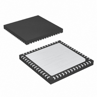
... RFID Readers Ordering Information PART* PIN-PACKAGE MAX19712ETN 56 Thin QFN-EP** MAX19712ETN+ 56 Thin QFN-EP** * All devices are specified over the -40°C to +85°C operating range Exposed paddle. + Denotes lead-free package. ________________________________________________________________ Maxim Integrated Products For pricing, delivery, and ordering information, please contact Maxim/Dallas Direct! at 1-888-629-4642, or visit Maxim’ ...
Page 2
Full-Duplex Analog Front-End ABSOLUTE MAXIMUM RATINGS GND OGND ..............................-0.3V to +3.6V GND to OGND.......................................................-0.3V to +0.3V IAP, IAN, QAP, QAN, IDP, IDN, QDP, QDN, DAC1, DAC2, DAC3 to GND .....................-0. ...
Page 3
ELECTRICAL CHARACTERISTICS (continued 3V 1.8V, internal reference (1.024V amplitude = -0.5dBFS, Tx DAC output amplitude = 0dBFS, CM1 = 0, CM0 = 0, differential Rx ADC input, differential Tx DAC output ...
Page 4
Full-Duplex Analog Front-End ELECTRICAL CHARACTERISTICS (continued 3V 1.8V, internal reference (1.024V amplitude = -0.5dBFS, Tx DAC output amplitude = 0dBFS, CM1 = 0, CM0 = 0, differential Rx ADC input, differential ...
Page 5
ELECTRICAL CHARACTERISTICS (continued 3V 1.8V, internal reference (1.024V amplitude = -0.5dBFS, Tx DAC output amplitude = 0dBFS, CM1 = 0, CM0 = 0, differential Rx ADC input, differential Tx DAC output ...
Page 6
Full-Duplex Analog Front-End ELECTRICAL CHARACTERISTICS (continued 3V 1.8V, internal reference (1.024V amplitude = -0.5dBFS, Tx DAC output amplitude = 0dBFS, CM1 = 0, CM0 = 0, differential Rx ADC input, differential ...
Page 7
ELECTRICAL CHARACTERISTICS (continued 3V 1.8V, internal reference (1.024V amplitude = -0.5dBFS, Tx DAC output amplitude = 0dBFS, CM1 = 0, CM0 = 0, differential Rx ADC input, differential Tx DAC output ...
Page 8
Full-Duplex Analog Front-End ELECTRICAL CHARACTERISTICS (continued 3V 1.8V, internal reference (1.024V amplitude = -0.5dBFS, Tx DAC output amplitude = 0dBFS, CM1 = 0, CM0 = 0, differential Rx ADC input, differential ...
Page 9
ELECTRICAL CHARACTERISTICS (continued 3V 1.8V, internal reference (1.024V amplitude = -0.5dBFS, Tx DAC output amplitude = 0dBFS, CM1 = 0, CM0 = 0, differential Rx ADC input, differential Tx DAC output ...
Page 10
Full-Duplex Analog Front-End ( 1.8V, internal reference (1.024V amplitude = -0.5dBFS, Tx DAC output amplitude = 0dBFS, CM1 = 0, CM0 = 0, differential Rx ADC input, differential Tx DAC output, ...
Page 11
OV = 1.8V, internal reference (1.024V amplitude = -0.5dBFS, Tx DAC output amplitude = 0dBFS, CM1 = 0, CM0 = 0, differential Rx ADC input, differential Tx DAC output ...
Page 12
Full-Duplex Analog Front-End ( 1.8V, internal reference (1.024V amplitude = -0.5dBFS, Tx DAC output amplitude = 0dBFS, CM1 = 0, CM0 = 0, differential Rx ADC input, differential Tx DAC output, ...
Page 13
OV = 1.8V, internal reference (1.024V amplitude = -0.5dBFS, Tx DAC output amplitude = 0dBFS, CM1 = 0, CM0 = 0, differential Rx ADC input, differential Tx DAC output ...
Page 14
Full-Duplex Analog Front-End ( 1.8V, internal reference (1.024V amplitude = -0.5dBFS, Tx DAC output amplitude = 0dBFS, CM1 = 0, CM0 = 0, differential Rx ADC input, differential Tx DAC output, ...
Page 15
PIN NAME Positive Reference Voltage Input Terminal. Bypass with a 0.33µF capacitor to GND as close to REFP 1 REFP as possible 11, 39, Analog Supply Voltage. Bypass 41, 47 0.1µF capacitor. 3 ...
Page 16
Full-Duplex Analog Front-End The MAX19712 integrates three 12-bit auxiliary DACs (aux-DACs) and a 10-bit, 333ksps auxiliary ADC (aux- ADC) with 4:1 input multiplexer. The aux-DAC channels feature 1µs settling time for fast AGC, VGA, and AFC level setting. ...
Page 17
Table 1. Rx ADC Output Codes vs. Input Voltage DIFFERENTIAL INPUT DIFFERENTIAL INPUT (LSB) VOLTAGE V x 512/512 511 (+Full Scale - 1 LSB) REF V x 511/512 510 (+Full Scale - 2 LSB) REF V x 1/512 REF V ...
Page 18
Full-Duplex Analog Front-End CLK CLK t t DOQ DOI D0–D9 D0Q D1I D1Q Figure 3. Rx ADC System Timing Diagram Table 2. Tx DAC Output Voltage vs. Input Codes (Internal Reference ...
Page 19
Tx DAC CH-ID Tx DAC CH-QD FULL SCALE = 1.56V V = 1.36V COMD ZERO SCALE = 1.16V 0V Figure 4. Tx DAC Common-Mode DC Level at IDN, IDP or QDN, QDP Differential Outputs CLK t DSQ D0– ...
Page 20
Full-Duplex Analog Front-End Figure 5 shows the relationship among the clock, input data, and analog outputs. Channel ID data is latched on the falling edge of the clock signal, and channel QD data is latched on the rising ...
Page 21
Table 3. MAX19712 Mode Control D11 D10 REGISTER NAME (MSB) 15 E11 = 0 E10 = 0 ENABLE-16 Reserved Reserved Aux-DAC1 1D11 1D10 Aux-DAC2 2D11 2D10 Aux-DAC3 3D11 3D10 IOFFSET — — QOFFSET — — COMSEL — — AD11 = ...
Page 22
Full-Duplex Analog Front-End Table 5. MAX19712 Tx, Rx, and FD Control Using SPI Commands ADDRESS DATA BITS 0000 (16-Bit Mode) and 1000 ...
Page 23
Table 6. MAX19712 Default (Power-On) Register Settings D11 D10 D9 REGISTER 16 NAME 15 14 (MSB) ENABLE- Aux Aux-DAC1 0 0 Aux-DAC2 0 0 Aux-DAC3 IOFFSET — — — QOFFSET — — ...
Page 24
Full-Duplex Analog Front-End Table 9. Offset Control Bits for ID and QD Channels (IOFFSET or QOFFSET Mode) BITS IO5–IO0 WHEN IN IOFFSET MODE, BITS QO5–QO0 WHEN IN QOFFSET MODE IO5/QO5 IO4/QO4 • ...
Page 25
CS/WAKE t CSS SCLK t DS MSB DIN Figure 6. Serial-Interface Timing Diagram CS/WAKE SCLK DIN AD0–AD9 ID/QD Figure 7. Mode-Recovery Timing Diagram MAX19712 enters the power mode determined by the WAKEUP-SEL register, however, all other settings (Tx DAC offset, ...
Page 26
Full-Duplex Analog Front-End System Clock Input (CLK) Both the Rx ADC and Tx DAC share the CLK input. The CLK input accepts a CMOS-compatible signal level set by OV from 1. Since the interstage con- ...
Page 27
Table 12. Auxiliary ADC Convert AD0 SELECTION 0 Aux-ADC Idle (Default) 1 Aux-ADC Start-Convert Table 13. Auxiliary ADC Reference AD1 SELECTION 0 Internal 2.048V Reference (Default) 1 Internal V Table 14. Auxiliary ADC Input Source AD3 AD2 Aux-ADC INPUT SOURCE ...
Page 28
Full-Duplex Analog Front-End The fastest method to perform sequential conversions with the aux-ADC is by sending consecutive commands setting AD10 = 1, AD0 = 1. With this sequence the CS/WAKE falling edge shifts data from the previous con- ...
Page 29
DIN can be written independent of DOUT state. A 16-bit instruction at DIN updates the device configuration. To prevent modifying internal registers while reading data from DOUT, hold DIN at a high state (only applies if sequential aux-ADC conversions are ...
Page 30
Full-Duplex Analog Front-End pared to single-ended mode. Figure 10 shows an RF transformer converting the MAX19712 Tx DAC differen- tial analog outputs to single-ended. Using Op-Amp Coupling Drive the MAX19712 Rx ADC with op amps when a balun ...
Page 31
R1 600Ω R2 600Ω R3 600Ω Figure 12. Rx ADC DC-Coupled Differential Drive Multilayer boards with separated ground and power planes yield the highest level of signal integrity. Use a split ground plane arranged to match the physical loca- tion ...
Page 32
Full-Duplex Analog Front-End IAP IAN MAX2392 QAP ZIF RECEIVER AGC QAN IDP MAX2395 IDN DIRECT MODULATOR QDP VGA PA DETECT QDN DAC1 TCXO DAC2 DAC3 ADC1 TEMPERATURE MEASUREMENT ADC2 Figure 13. Typical WCDMA Application Circuit 32 32 ______________________________________________________________________________________ ...
Page 33
Differential Nonlinearity (DNL) Differential nonlinearity is the difference between an actual step width and the ideal value of 1 LSB. A DNL error specification of less than 1 LSB guarantees no missing codes (ADC) and a monotonic transfer function (ADC ...
Page 34
Full-Duplex Analog Front-End Effective Number of Bits (ENOB) ENOB specifies the dynamic performance of an ADC at a specific input frequency and sampling rate. An ideal ADC’s error consists of quantization noise only. ENOB for a full-scale sinusoidal ...
Page 35
Full-Duplex V = 2.7V TO 3.3V DD IAP 10-BIT ADC IAN QAP 10-BIT ADC QAN IDP 10-BIT DAC IDN QDP 10-BIT DAC QDN PROGRAMMABLE OFFSET/CM 12-BIT DAC1 AUX-DAC 12-BIT DAC2 AUX-DAC 12-BIT DAC3 AUX-DAC ADC1 ADC2 AUX-ADC V ...
Page 36
... Maxim cannot assume responsibility for use of any circuitry other than circuitry entirely embodied in a Maxim product. No circuit patent licenses are implied. Maxim reserves the right to change the circuitry and specifications without notice at any time. 36 ____________________Maxim Integrated Products, 120 San Gabriel Drive, Sunnyvale, CA 94086 408-737-7600 © 2006 Maxim Integrated Products ...