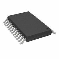
AD7367BRUZ-5 Analog Devices Inc, AD7367BRUZ-5 Datasheet - Page 7

AD7367BRUZ-5
Manufacturer Part Number
AD7367BRUZ-5
Description
IC ADC 14BIT DUAL 500KSPS 24-TSS
Manufacturer
Analog Devices Inc
Datasheet
1.AD7367BRUZ-5.pdf
(28 pages)
Specifications of AD7367BRUZ-5
Data Interface
DSP, MICROWIRE™, QSPI™, Serial, SPI™
Design Resources
Driving the AD7366/7 Bipolar SAR ADC in Low-Distortion DC-Coupled Appls (CN0042)
Number Of Bits
14
Sampling Rate (per Second)
500k
Number Of Converters
2
Power Dissipation (max)
88.8mW
Voltage Supply Source
Analog and Digital, Dual ±
Operating Temperature
-40°C ~ 85°C
Mounting Type
Surface Mount
Package / Case
24-TSSOP (0.173", 4.40mm Width)
Resolution (bits)
14bit
Input Channel Type
Single Ended
Supply Voltage Range - Analogue
4.75V To 5.25V, ± 11.5V To ± 16.5V
Supply Voltage Range - Digital
2.7V To
Sampling Rate
1MSPS
Rohs Compliant
Yes
Lead Free Status / RoHS Status
Lead free / RoHS Compliant
For Use With
EVAL-AD7367CBZ - BOARD EVALUATION FOR AD7367
Lead Free Status / RoHS Status
Lead free / RoHS Compliant, Lead free / RoHS Compliant
Available stocks
Company
Part Number
Manufacturer
Quantity
Price
Company:
Part Number:
AD7367BRUZ-5
Manufacturer:
ADI
Quantity:
1 000
Company:
Part Number:
AD7367BRUZ-5-RL7
Manufacturer:
ADI
Quantity:
1 000
TIMING SPECIFICATIONS
AV
Table 4.
Parameter
t
f
t
t
t
t
t
t
t
t
t
t
t
1
2
SCLK
CONVERT
QUIET
1
2
3
4
5
6
7
8
9
POWER-UP
Sample tested during initial release to ensure compliance. All input signals are specified with t
The time required for the output to cross is 0.4 V or 2.4 V.
All timing specifications given are with a 25 pF load capacitance. With a load capacitance greater than this value, a digital buffer or latch must be used. See the
Terminology section and Figure 25.
2
CC
= DV
CC
= 4.75 V to 5.25 V; V
2.7 V ≤ V
1.25
1.25
10
20
50
10
40
0
10
20
7
0.3 × t
0.3 × t
10
70
SCLK
SCLK
DRIVE
≤ 5.25 V
DD
= 5 V to 16.5 V; V
Unit
μs max
μs max
kHz min
MHz max
ns min
ns min
ns min
ns min
ns max
ns max
ns min
ns min
ns min
ns max
μs max
Test Conditions/Comments
Conversion time, internal clock. CONVST falling edge to BUSY falling edge.
For the AD7367-5.
For the AD7366-5.
Frequency of serial read clock.
Minimum quiet time required between the end of serial read and the start of the next
conversion.
Minimum CONVST low pulse.
CONVST falling edge to BUSY rising edge.
BUSY falling edge to MSB valid once CS is low for t
Delay from CS falling edge until Pin 1 (D
Data access time after SCLK falling edge.
SCLK to data valid hold time.
SCLK low pulse width.
SCLK high pulse width.
CS rising edge to D
Power up time from shutdown mode; time required between CONVST rising edge and
CONVST falling edge.
SS
= −16.5 V to −5 V; V
Rev. A | Page 7 of 28
OUT
A, D
DRIVE
OUT
R
= 2.7 V to 5.25 V; T
B, high impedance.
= t
F
= 5 ns (10% to 90% of V
OUT
A) and Pin 23 (D
A
= T
4
prior to BUSY going low.
DRIVE
MIN
) and timed from a voltage level of 1.6 V.
AD7366-5/AD7367-5
to T
OUT
MAX
B) are three-state disabled.
, unless otherwise noted.
1


