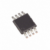
MAX11607EUA+ Maxim Integrated Products, MAX11607EUA+ Datasheet - Page 17

MAX11607EUA+
Manufacturer Part Number
MAX11607EUA+
Description
IC ADC SERIAL 10BIT 4CH 8-MSOP
Manufacturer
Maxim Integrated Products
Datasheet
1.MAX11607EUA.pdf
(22 pages)
Specifications of MAX11607EUA+
Number Of Bits
10
Sampling Rate (per Second)
94.4k
Data Interface
I²C, Serial
Number Of Converters
1
Power Dissipation (max)
2.2mW
Voltage Supply Source
Single Supply
Operating Temperature
-40°C ~ 85°C
Mounting Type
Surface Mount
Package / Case
8-TSSOP, 8-MSOP (0.118", 3.00mm Width)
Resolution
10 bit
Interface Type
I2C
Snr
60 dB
Voltage Reference
2.048 V
Supply Voltage (max)
3.6 V
Supply Voltage (min)
2.7 V
Maximum Power Dissipation
470.6 mW
Maximum Operating Temperature
+ 85 C
Mounting Style
SMD/SMT
Input Voltage
3.3 V
Minimum Operating Temperature
- 40 C
Lead Free Status / RoHS Status
Lead free / RoHS Compliant
Table 5. Scanning Configuration
* When operating in external clock mode, there is no difference between SCAN[1:0] = 01 and SCAN[1:0] = 11, and converting occurs
When configured for external clock mode (CLK = 1),
the MAX11606–MAX11611 use the SCL as the conver-
sion clock. In external clock mode, the MAX11606–
MAX11611 begin tracking the analog input on the ninth
rising clock edge of a valid slave address byte. Two
SCL clock cycles later the analog signal is acquired
and the conversion begins. Unlike internal clock mode,
converted data is available immediately after the first
four empty high bits. The device continuously converts
input channels dictated by the scan mode until given a
not acknowledge. There is no need to re-address the
device with a read command to obtain new conversion
results (see Figure 11).
The conversion must complete in 1ms or droop on the
track-and-hold capacitor degrades conversion results.
Use internal clock mode if the SCL clock period
exceeds 60µs.
The MAX11606–MAX11611 must operate in external
clock mode for conversion rates from 40ksps to
94.4ksps. Below 40ksps internal clock mode is recom-
mended due to much smaller power consumption.
SCAN0 and SCAN1 of the configuration byte set the
scan mode configuration. Table 5 shows the scanning
configurations. If AIN_/REF is set to be a reference input
or output (SEL1 = 1, Table 6), AIN_/REF is excluded
SCAN1
perpetually until not acknowledge occurs.
0
0
1
1
SCAN0
0
1
0
1
______________________________________________________________________________________
Scans up from AIN0 to the input selected by CS3–CS0. When CS3–CS0 exceeds 1011, the scanning stops at
AIN11. When AIN_/REF is set to be a REF input/output, scanning stops at AIN2 or AIN10.
*Converts the input selected by CS3–CS0 eight times (see Tables 3 and 4).
MAX11606/MAX11607: Scans upper half of channels.
Scans up from AIN2 to the input selected by CS1 and CS0. When CS1 and CS0 are set for AIN0, AIN1, and
AIN2, the only scan that takes place is AIN2 (MAX11606/MAX11607). When AIN/REF is set to be a REF
input/output, scanning stops at AIN2.
MAX11608/MAX11609: Scans upper quartile of channels.
Scans up from AIN6 to the input selected by CS3–CS0. When CS3–CS0 is set for AIN0–AIN6, the only scan
that takes place is AIN6 (MAX11608/MAX11609).
MAX11610/MAX11611: Scans upper half of channels.
Scans up from AIN6 to the input selected by CS3–CS0. When CS3–CS0 is set for AIN0–AIN6, the only scan
that takes place is AIN6 (MAX11610/MAX11611). When AIN/REF is set to be a REF input/output, scanning
stops at selected channel or AIN10.
*Converts channel selected by CS3–CS0.
10-Bit ADCs in Ultra-Small Packages
Low-Power, 4-/8-/12-Channel, I
External Clock
Scan Mode
SCANNING CONFIGURATION
from a multichannel scan. The scanned results are writ-
ten to memory in the same order as the conversion. Read
the results from memory in the order they were convert-
ed. Each result needs a 2-byte transmission, the first byte
begins with six empty bits during which SDA is left high.
Each byte has to be acknowledged by the master or the
memory transmission is terminated. It is not possible to
read the memory independently of conversion.
The configuration and setup registers (Tables 1 and 2)
default to a single-ended, unipolar, single-channel con-
version on AIN0 using the internal clock with V
reference and AIN_/REF configured as an analog input.
The memory contents are unknown after power-up.
Automatic shutdown occurs between conversions when
the MAX11606–MAX11611 are idle. All analog circuits
participate in automatic shutdown except the internal
reference due to its prohibitively long wake-up time.
When operating in external clock mode, a STOP, not-
acknowledge or repeated START, condition must be
issued to place the devices in idle mode and benefit
from automatic shutdown. A STOP condition is not nec-
essary in internal clock mode to benefit from automatic
shutdown because power-down occurs once all con-
version results are written to memory (Figure 10). When
Applications Information
Automatic Shutdown
Power-On Reset
DD
2
as the
C,
17


