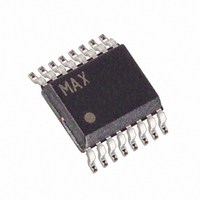
MAX1038AEEE+ Maxim Integrated Products, MAX1038AEEE+ Datasheet - Page 12

MAX1038AEEE+
Manufacturer Part Number
MAX1038AEEE+
Description
IC ADC 8-BIT 188KSPS 16-QSOP
Manufacturer
Maxim Integrated Products
Datasheet
1.MAX1037EKAT.pdf
(23 pages)
Specifications of MAX1038AEEE+
Number Of Bits
8
Sampling Rate (per Second)
188k
Data Interface
I²C, Serial
Number Of Converters
1
Power Dissipation (max)
1.75mW
Voltage Supply Source
Single Supply
Operating Temperature
-40°C ~ 85°C
Mounting Type
Surface Mount
Package / Case
16-SSOP (0.150", 3.90mm Width)
Number Of Adc Inputs
12
Architecture
SAR
Conversion Rate
188 KSPs
Resolution
8 bit
Input Type
Differential
Interface Type
Serial (2-Wire, I2C)
Voltage Reference
Internal 4.096 V or External
Supply Voltage (max)
5.5 V
Supply Voltage (min)
4.5 V
Maximum Power Dissipation
666.7 mW
Maximum Operating Temperature
+ 85 C
Mounting Style
SMD/SMT
Minimum Operating Temperature
- 40 C
Lead Free Status / RoHS Status
Lead free / RoHS Compliant
SCL is high (Figure 5). A repeated START condition (Sr)
can be used in place of a STOP condition to leave the
bus active and in its current timing mode (see the HS-
Mode section).
Successful data transfers are acknowledged with an
acknowledge bit (A) or a not-acknowledge bit (A). Both
the master and the MAX1036–MAX1039 (slave) generate
acknowledge bits. To generate an “acknowledge,” the
receiving device must pull SDA low before the rising
edge of the acknowledge related clock pulse (ninth
pulse) and keep it low during the high period of the clock
pulse (Figure 6). To generate a “not acknowledge,” the
receiver allows SDA to be pulled high before the rising
edge of the acknowledge related clock pulse and leaves
it high during the high period of the clock pulse.
Monitoring the acknowledge bits allows for detection of
unsuccessful data transfers. An unsuccessful data
transfer happens if a receiving device is busy or if a
system fault has occurred. In the event of an unsuc-
cessful data transfer, the bus master should reattempt
communication at a later time.
A bus master initiates communication with a slave
device by issuing a START condition followed by a
slave address. When idle, the MAX1036–MAX1039 con-
tinuously wait for a START condition followed by their
slave address. When the MAX1036–MAX1039 recog-
nize their slave address, they are ready to accept or
send data. The slave address has been factory pro-
grammed and is always 1100100 for the MAX1036/
MAX1037, and 1100101 for MAX1038/ MAX1039
(Figure 7). The least significant bit (LSB) of the address
byte (R/W) determines whether the master is writing to
or reading from the MAX1036–MAX1039 (R/W = zero
selects a write condition. R/W = 1 selects a read condi-
tion). After receiving the address, the MAX1036–
MAX1039 (slave) issue an acknowledge by pulling SDA
low for one clock cycle.
At power-up, the MAX1036–MAX1039 bus timing
defaults to fast mode (F/S-mode) allowing conversion
rates up to 44ksps. The MAX1036–MAX1039 must
operate in high-speed mode (HS-mode) to achieve
conversion rates up to 188ksps. Figure 1 shows the bus
timing for the MAX1036–MAX1039’s 2-wire interface.
At power-up, the MAX1036–MAX1039 bus timing is set
for F/S-mode. The master selects HS-mode by address-
ing all devices on the bus with the HS-mode master
2.7V to 3.6V and 4.5V to 5.5V, Low-Power,
4-/12-Channel 2-Wire Serial 8-Bit ADCs
12
______________________________________________________________________________________
Acknowledge Bits
Slave Address
Bus Timing
HS-Mode
code 0000 1XXX (X = Don’t care). After successfully
receiving the HS-mode master code, the MAX1036–
MAX1039 issues a not acknowledge, allowing SDA to be
pulled high for one clock cycle (Figure 8). After the not
acknowledge, the MAX1036–MAX1039 are in HS-mode.
The master must then send a repeated START followed
by a slave address to initiate HS-mode communication. If
the master generates a STOP condition, the
MAX1036–MAX1039 return to F/S-mode.
Write cycles begin with the master issuing a START
condition followed by 7 address bits (Figure 7) and 1
write bit (R/W = zero). If the address byte is successful-
ly received, the MAX1036–MAX1039 (slave) issue an
acknowledge. The master then writes to the slave. The
slave recognizes the received byte as the setup byte
(Table 1) if the most significant bit (MSB) is 1. If the
MSB is zero, the slave recognizes that byte as the con-
figuration byte (Table 2). The master can write either 1
or 2 bytes to the slave in any order (setup byte then
configuration byte; configuration byte then setup byte;
setup byte only; configuration byte only; Figure 9). If the
slave receives bytes successfully, it issues an acknowl-
edge. The master ends the write cycle by issuing a
STOP condition or a repeated START condition. When
operating in HS-mode, a STOP condition returns the
bus to F/S-mode (see the HS-Mode section).
A read cycle must be initiated to obtain conversion
results. Read cycles begin with the bus master issuing
Figure 5. START and STOP Conditions
Figure 6. Acknowledge Bits
SDA
SDA
SCL
SCL
S
S
Configuration/Setup Bytes (Write Cycle)
1
2
Sr
Data Byte (Read Cycle)
NOT ACKNOWLEDGE
ACKNOWLEDGE
8
P
9


