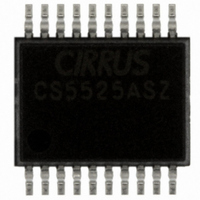
CS5525-ASZ Cirrus Logic Inc, CS5525-ASZ Datasheet - Page 18

CS5525-ASZ
Manufacturer Part Number
CS5525-ASZ
Description
IC ADC 16BIT W/4BIT LATCH 20SSOP
Manufacturer
Cirrus Logic Inc
Datasheet
1.CS5526-BSZ.pdf
(30 pages)
Specifications of CS5525-ASZ
Number Of Converters
1
Package / Case
20-SSOP
Number Of Bits
16
Data Interface
Serial
Power Dissipation (max)
12.7mW
Voltage Supply Source
Analog and Digital
Operating Temperature
-40°C ~ 85°C
Mounting Type
Surface Mount
Number Of Adc Inputs
1
Architecture
Delta-Sigma
Conversion Rate
3.76 SPs to 616 SPs
Resolution
16 bit
Input Type
Voltage
Interface Type
Serial (3-Wire)
Voltage Reference
2.5 V
Supply Voltage (max)
5 V
Supply Voltage (min)
25 mV
Maximum Power Dissipation
500 mW
Maximum Operating Temperature
+ 85 C
Mounting Style
SMD/SMT
Input Voltage
25 mV to 5 V
Minimum Operating Temperature
- 40 C
Lead Free Status / RoHS Status
Lead free / RoHS Compliant
For Use With
598-1013 - EVAL BOARD FOR CS5525
Lead Free Status / Rohs Status
Lead free / RoHS Compliant
Other names
598-1107-5
Available stocks
Company
Part Number
Manufacturer
Quantity
Price
Part Number:
CS5525-ASZ
Manufacturer:
CIRRUS
Quantity:
20 000
VREF- as shown in Figure 12. For any input range
other than the 2.5 V range, the modulator gain error
can not be completely calibrated out. This is due to
the lack of an accurate full scale voltage internal to
the chips. The 2.5 V range is an exception because
the external reference voltage is 2.5 V nominal and
is used as the full scale voltage. In addition, when
self-calibration of gain is performed in the 25 mV,
55 mV, and 100 mV input ranges, the instrumenta-
tion amplifier’s gain is not calibrated. These two
factors can leave the converters with a gain error of
up to ±20% after self-calibration of gain. There-
fore, a system gain is required to get better accura-
cy, except for the 2.5 V range.
System Calibration
For the system calibration functions, the user must
supply the converters calibration signals which rep-
resent ground and full scale. When a system offset
calibration is performed, a ground reference signal
must be applied to the converter. See Figures 13
and 14. As shown in Figures 15 and 16, the user
must input a signal representing the positive full
scale point to perform a system gain calibration. In
either case, the calibration signals must be within
the specified calibration limits for each specific
calibration step (refer to the System Calibration
Specifications).
18
Reference
Figure 12. Self Calibration of Gain (All Ranges).
+
-
VREF+
VREF-
AIN+
AIN-
+
-
X20
CLOSED
CLOSED
OPEN
OPEN
+
-
Figure 13. System Calibration of Offset (Low Ranges).
Figure 14. System Calibration of Offset (High Ranges).
Full Scale + -
Full Scale
Figure 16. System Calibration of Gain (High Ranges).
Figure 15. System Calibration of Gain (Low Ranges)
CM + -
CM
CM + -
0V + -
CM + -
0V
External
Connections
External
Connections
External
Connections
+
+
-
-
External
Connections
+
-
AIN+
AIN-
AIN+
AIN+
AIN-
AIN-
AIN+
AIN-
CS5525 CS5526
+
-
+
-
+
-
+
-
X20
X20
X20
X20
DS202F5
+
-
+
-
+
-
+
-


