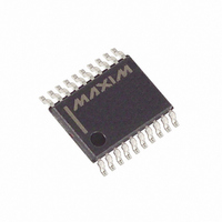
MAX1146BCUP+ Maxim Integrated Products, MAX1146BCUP+ Datasheet - Page 16

MAX1146BCUP+
Manufacturer Part Number
MAX1146BCUP+
Description
IC ADC 14BIT 116KSPS 20-TSSOP
Manufacturer
Maxim Integrated Products
Datasheet
1.MAX1147BEUP.pdf
(25 pages)
Specifications of MAX1146BCUP+
Number Of Bits
14
Sampling Rate (per Second)
116k
Data Interface
MICROWIRE™, QSPI™, Serial, SPI™
Number Of Converters
1
Power Dissipation (max)
879mW
Voltage Supply Source
Single Supply
Operating Temperature
0°C ~ 70°C
Mounting Type
Surface Mount
Package / Case
20-TSSOP
Lead Free Status / RoHS Status
Lead free / RoHS Compliant
Multichannel, True-Differential,
Serial, 14-Bit ADCs
In unipolar input mode, the digital output is straight
binary (Figure 14). For bipolar input mode, the digital
output is two’s complement binary (Figure 15). Data is
clocked out on the falling edge of SCLK in MSB-first
format.
The MAX1146–MAX1149 can use either the external
serial clock or the internal clock to drive the succes-
sive-approximation conversion. The external clock
shifts data in and out of the MAX1146–MAX1149.
External clock mode allows the fastest throughput rate
(116ksps) and serial clock frequencies from 0.1MHz to
2.1MHz. Internal clock mode provides the best noise
performance because the digital interface can be idle
during conversion. The internal clock mode serial clock
frequency can range from 0 to 2.1MHz. Internal clock
mode allows the CPU to request a conversion and
clock back the results.
Bits PD1 and PD0 of the control byte program the clock
and power-down modes. The MAX1146–MAX1149 power
up in internal clock mode with all circuits activated.
Figures 8–11 illustrate the available clocking modes.
In external clock mode, the external clock not only
shifts data in and out, but it also drives the analog-to-
digital conversion. SSTRB pulses high for two clock
periods after the last bit of the control byte. Successive-
approximation bit decisions are made and the results
appear at DOUT on each of the next 14 SCLK falling
edges (Figures 8 and10). SSTRB and DOUT go into a
high-impedance state when CS is high.
Figure 8. External Clock Mode—24 Clocks/Conversion Timing
16
INPUT MUX
INPUT T/H
SSTRB
DOUT
SCLK
______________________________________________________________________________________
DIN
CS
SET ACCORDING TO PREVIOUS CONTROL BYTE
HIGH-Z
HIGH-Z
START SEL2
1
SEL1 SEL0
TRACK
CB1
SGL/DIF UNI/BIP
SET TO CB1
t
PD1
ACQ
PD0
8
Clock Modes
External Clock
Digital Output
9
OPEN
D13 D12 D11 D10
D9
t
CONV
D8
Use internal clock mode if the serial clock frequency is
less than 100kHz or if serial clock interruptions could
cause the conversion interval to exceed 140µs. The
conversion must complete in 140µs, or droop on the
T/H capacitors can degrade conversion results.
When configured for internal clock mode, the
MAX1146–MAX1149 generate an internal conversion
clock. This frees the µP from the burden of running the
SAR conversion clock and allows the conversion results
to be read back at the processor’s convenience, at any
clock rate up to 2.1MHz. SSTRB goes low at the start of
the conversion and then goes high when the conver-
sion is complete. SSTRB is low for a maximum of 8.0µs,
during which time SCLK should remain low for best
noise performance.
An internal register stores data when the conversion is in
progress. SCLK clocks the data out of this register at any
time after the conversion is complete. After SSTRB goes
high, the second falling SCLK clock edge produces the
MSB of the conversion at DOUT, followed by the remain-
ing bits in MSB-first format (Figures 9 and 11).
For the most accurate conversion, the MAX1146–
MAX1149 digital I/O should remain inactive during the
internal clock conversion interval (t
CS high during conversion. Pulling CS high aborts the
current conversion. To ensure that the next start bit is
recognized, clock in 18 zeros at DIN. When internal
clock mode is selected, SSTRB does not go into a high-
impedance state when CS goes high. A rising edge on
SSTRB indicates that the MAX1146–MAX1149 have fin-
ished the conversion. The µP can then read the conver-
sion results at its convenience.
16
HOLD
D7
D6
D5
D4
D3
D2
D1
D0
24
CONV
RESET TO CB1
TRACK
Internal Clock
). Do not pull
HIGH-Z
HIGH-Z


