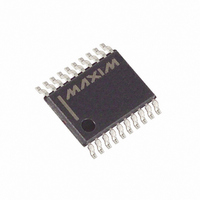
MAX1147BCUP+ Maxim Integrated Products, MAX1147BCUP+ Datasheet - Page 15

MAX1147BCUP+
Manufacturer Part Number
MAX1147BCUP+
Description
IC ADC 14BIT 116KSPS 20-TSSOP
Manufacturer
Maxim Integrated Products
Datasheet
1.MAX1147BEUP.pdf
(25 pages)
Specifications of MAX1147BCUP+
Number Of Bits
14
Sampling Rate (per Second)
116k
Data Interface
MICROWIRE™, QSPI™, Serial, SPI™
Number Of Converters
1
Power Dissipation (max)
879mW
Voltage Supply Source
Single Supply
Operating Temperature
0°C ~ 70°C
Mounting Type
Surface Mount
Package / Case
20-TSSOP
Lead Free Status / RoHS Status
Lead free / RoHS Compliant
When power is first applied, internal power-on reset cir-
cuitry activates the MAX1146–MAX1149 in internal
clock mode, making the MAX1146–MAX1149 ready to
convert with SSTRB high. No conversions should be
performed until the power supply is stable. The first log-
ical 1 on DIN with CS low is interpreted as a start bit.
Until a conversion takes place, DOUT shifts out zeros.
Start a conversion by clocking a control byte into DIN.
With CS low, a rising edge on SCLK latches a bit from
DIN into the MAX1146–MAX1149 internal shift register.
After CS falls, the first logic 1 bit defines the control
Table 2. MAX1148/MAX1149 Channel Selection in Single-Ended Mode (SGL/DIF = 1)
Table 3. MAX1148/MAX1149 Channel Selection in Differential Mode (SGL/DIF = 0)
Table 4. MAX1146/MAX1147 Channel
Selection in Single-Ended Mode
(SGL/DIF = 1)
SEL2
SEL2
SEL2
0
1
0
1
0
1
0
1
0
1
0
1
0
0
0
0
1
1
1
1
SEL1
0
0
0
0
SEL1
SEL1
0
0
0
0
1
1
1
1
SEL0
0
0
1
1
0
0
1
1
0
0
1
1
______________________________________________________________________________________
SEL0
CH0
0
0
1
1
0
0
1
1
+
SEL0
0
1
0
1
0
1
0
1
Starting a Conversion
CH1
+
CH0
+
Power-On Reset
CH0
+
-
CH2
+
Multichannel, True-Differential,
CH1
+
CH3
+
CH1
+
-
COM
CH2
-
-
-
-
+
CH2
+
-
byte’s MSB. Until this start bit arrives, any number of
logic 0 bits can be clocked into DIN with no effect.
Table 1 shows the control-byte format.
The MAX1146–MAX1149 are compatible with SPI/QSPI
and MICROWIRE devices. For SPI, select the correct
clock polarity and sampling edge in the SPI control reg-
isters. Set CPOL = 0 and CPHA = 0. MICROWIRE, SPI,
and QSPI transmit a byte and receive a byte at the same
time. Using the Typical Application Circuit (Figure 4), the
simplest software interface requires only three 8-bit
transfers to perform a conversion (one 8-bit transfer to
configure the ADC, and two more 8-bit transfers to clock
out the 14-bit conversion result).
Table 5. MAX1146/MAX1147 Channel
Selection in Differential Mode
(SGL/DIF = 0)
CH3
SEL2
+
0
0
1
1
CH3
+
-
SEL1
Serial, 14-Bit ADCs
CH4
0
0
0
0
+
CH4
SEL0
+
-
0
1
0
1
CH5
+
CH0
+
CH5
-
+
-
CH6
+
CH1
+
-
CH6
CH7
+
-
+
CH2
+
-
CH7
COM
+
CH3
-
-
-
-
-
-
-
-
-
+
-
15


