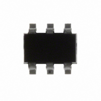
AD7940BRJZ-REEL7 Analog Devices Inc, AD7940BRJZ-REEL7 Datasheet - Page 3

AD7940BRJZ-REEL7
Manufacturer Part Number
AD7940BRJZ-REEL7
Description
IC ADC 14BIT 100KSPS SOT-23-6
Manufacturer
Analog Devices Inc
Datasheet
1.AD7940BRJZ-REEL7.pdf
(20 pages)
Specifications of AD7940BRJZ-REEL7
Data Interface
DSP, MICROWIRE™, QSPI™, Serial, SPI™
Number Of Bits
14
Sampling Rate (per Second)
100k
Number Of Converters
1
Power Dissipation (max)
26.4mW
Voltage Supply Source
Single Supply
Operating Temperature
-40°C ~ 85°C
Mounting Type
Surface Mount
Package / Case
SOT-23-6
Resolution (bits)
14bit
Sampling Rate
100kSPS
Input Channel Type
Single Ended
Supply Voltage Range - Analog
2.5V To 5.5V
Supply Current
4.8mA
Lead Free Status / RoHS Status
Lead free / RoHS Compliant
For Use With
EVAL-AD7940CBZ - BOARD EVALUATION AD7940AD7940-DBRD - BOARD EVAL FOR AD7940 STAMP SPI
Lead Free Status / RoHS Status
Lead free / RoHS Compliant, Lead free / RoHS Compliant
Other names
AD7940BRJZ-REEL7
AD7940BRJZ-REEL7TR
AD7940BRJZ-REEL7TR
Available stocks
Company
Part Number
Manufacturer
Quantity
Price
Company:
Part Number:
AD7940BRJZ-REEL7
Manufacturer:
ADI
Quantity:
1 000
SPECIFICATIONS
V
Table 2.
Parameter
DYNAMIC PERFORMANCE
DC ACCURACY
ANALOG INPUT
LOGIC INPUTS
LOGIC OUTPUTS
CONVERSION RATE
POWER REQUIREMENTS
DD
Signal-to-Noise + Distortion (SINAD)
Total Harmonic Distortion (THD)
Peak Harmonic or Spurious Noise (SFDR)
Intermodulation Distortion (IMD)
Aperture Delay
Aperture Jitter
Full Power Bandwidth
Resolution
Integral Nonlinearity
Offset Error
Gain Error
Input Voltage Ranges
DC Leakage Current
Input Capacitance
Input High Voltage, V
Input Low Voltage, V
Input Current, I
Input Capacitance, C
Output High Voltage, V
Output Low Voltage, V
Floating-State Leakage Current
Floating-State Output Capacitance
Output Coding
Conversion Time
Track-and-Hold Acquisition Time
Throughput Rate
V
I
DD
DD
= 2.50 V to 5.5 V, f
Second-Order Terms
Third-Order Terms
Normal Mode (Static)
Normal Mode (Operational)
Full Power-Down Mode
2
2
IN
SCLK
2
IN
INL
INH
2, 3
OL
OH
1
= 2.5 MHz, f
2
2
2, 3
2
SAMPLE
2
= 100 kSPS, unless otherwise noted; T
B Version
81
−98
−95
−94
−100
20
30
7
2
14
13
±1
±2
±6
±8
0 to V
±0.3
30
2.4
0.4
0.8
±0.3
10
V
0.4
±0.3
10
8
500
400
100
2.50/5.5
5.2
2
4.8
1.9
0.5
0.3
DD
– 0.2
Straight (Natural) Binary
DD
Rev. 0 | Page 3 of 20
1
Unit
dB min
dB typ
dB typ
dB typ
dB typ
ns max
ps typ
MHz typ
MHz typ
Bits min
Bits min
LSB max
LSB max
LSB max
LSB max
V
µA max
pF typ
V min
V max
V max
µA max
pF max
V min
V max
µA max
pF max
µs max
ns max
ns max
kSPS max
V min/V max
mA max
mA max
mA max
mA max
µA max
µA max
A
= T
MIN
Test Conditions/Comments
f
@ −3 dB
@ −0.1 dB
V
V
V
V
V
V
Typically 10 nA, V
I
I
16 SCLK cycles
Full-scale step input
Sine wave input ≤ 10 kHz
See the Serial Interface section
Digital I/P
V
V
V
V
SCLK on or off. V
SCLK on or off. V
SOURCE
SINK
IN
DD
DD
DD
DD
DD
DD
DD
DD
DD
DD
= 10 kHz sine wave
to T
= 2.5 V to 4.096 V
> 4.096 V
= 2.5 V to 4.096 V
> 4.096 V
= 3 V
= 5 V
= 5.5 V; SCLK on or off
= 3.6 V; SCLK on or off
= 5.5 V; f
= 3.6 V; f
= 200 µA
= 200 µA; V
MAX
S
, unless otherwise noted.
= 0 V or V
SAMPLE
SAMPLE
DD
DD
IN
DD
= 100 kSPS; 3.3 mA typ
= 100 kSPS; 1.29 mA typ
= 5.5 V
= 3.6 V
= 0 V or V
= 2.50 V to 5.25 V
DD
DD
AD7940


