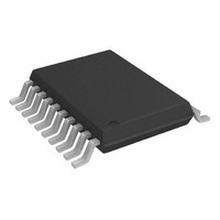
AD7927BRUZ Analog Devices Inc, AD7927BRUZ Datasheet - Page 15

AD7927BRUZ
Manufacturer Part Number
AD7927BRUZ
Description
IC ADC 12BIT 8CH 200KSPS 20TSSOP
Manufacturer
Analog Devices Inc
Specifications of AD7927BRUZ
Data Interface
DSP, MICROWIRE™, QSPI™, Serial, SPI™
Number Of Bits
12
Sampling Rate (per Second)
200k
Number Of Converters
1
Power Dissipation (max)
7.5mW
Voltage Supply Source
Single Supply
Operating Temperature
-40°C ~ 85°C
Mounting Type
Surface Mount
Package / Case
20-TSSOP (0.173", 4.40mm Width)
Resolution (bits)
12bit
Sampling Rate
200kSPS
Input Channel Type
Single Ended
Supply Voltage Range - Analog
2.7V To 5.25V
Supply Current
1.5mA
Number Of Elements
1
Resolution
12Bit
Architecture
SAR
Sample Rate
200KSPS
Input Polarity
Unipolar
Input Type
Voltage
Rated Input Volt
2.5/5V
Differential Input
No
Power Supply Requirement
Analog and Digital
Single Supply Voltage (typ)
3/5V
Single Supply Voltage (min)
2.7V
Single Supply Voltage (max)
5.25V
Dual Supply Voltage (typ)
Not RequiredV
Dual Supply Voltage (min)
Not RequiredV
Dual Supply Voltage (max)
Not RequiredV
Power Dissipation
7.5mW
Differential Linearity Error
-0.9LSB/1.5LSB
Integral Nonlinearity Error
±1LSB
Operating Temp Range
-40C to 85C
Operating Temperature Classification
Industrial
Mounting
Surface Mount
Pin Count
20
Package Type
TSSOP
Input Signal Type
Single-Ended
Lead Free Status / RoHS Status
Lead free / RoHS Compliant
For Use With
EVAL-AD7927CBZ - BOARD EVALUATION FOR AD7927
Lead Free Status / Rohs Status
Compliant
Available stocks
Company
Part Number
Manufacturer
Quantity
Price
Company:
Part Number:
AD7927BRUZ
Manufacturer:
ADI
Quantity:
1 000
Part Number:
AD7927BRUZ
Manufacturer:
ADI/亚德诺
Quantity:
20 000
Company:
Part Number:
AD7927BRUZ-REEL7
Manufacturer:
ADI
Quantity:
3
Company:
Part Number:
AD7927BRUZ-REEL7
Manufacturer:
ADI
Quantity:
1 000
CS
CS
CS
Figure 13. SEQ and SHADOW Conversion Flowchart to Convert a Sequence of
CIRCUIT INFORMATION
The AD7927 is a high speed, 8-channel, 12-bit, single-supply
ADC. The part can be operated from a 2.7 V to 5.25 V supply.
When operated from either a 5 V or 3 V supply, the AD7927 is
capable of throughput rates of 200 kSPS. The conversion time
may be as short as 800 ns when provided with a 20 MHz clock.
The AD7927 provides the user with an on-chip, track-and-hold
ADC and a serial interface housed in a 20-lead TSSOP. The
AD7927 has eight single-ended input channels with a channel
sequencer, allowing the user to select a channel sequence
through which the ADC can cycle with each consecutive CS
falling edge. The serial clock input accesses data from the part,
controls the transfer of data written to the ADC, and provides
the clock source for the successive approximation ADC. The
analog input range for the AD7927 is 0 V to REF
2 × REF
For the 0 to 2 × REF
4.75 V to 5.25 V supply.
The AD7927 provides flexible power management options
to allow the user to achieve the best power performance for a
given throughput rate. These options are selected by program-
ming the power management bits, PM1 and PM0, in the control
register.
IN
, depending on the status of Bit 1 in the control register.
CONTINUOUSLY CONVERTS ON THE SELECTED
SEQUENCE OF CHANNELS BUT ALLOWS
RANGE, CODING AND SO ON, TO CHANGE IN THE
CONTROL REGISTER WITHOUT INTERRUPTING
THE SEQUENCE, PROVIDED SEQ = 1, SHADOW = 0
DIN: WRITE TO CONTROL REGISTER,
WRITE BIT = 1,
SELECT CODING, RANGE, AND POWER MODE.
SELECT CHANNEL A2 TO CHANNEL A0
FOR CONVERSION.
SEQ = 1, SHADOW = 1
DOUT: CONVERSION RESULT FROM CHANNEL 0
CONTINUOUSLY CONVERTS ON A CONSECUTIVE
SEQUENCE OF CHANNELS FROM CHANNEL 0 UP
TO AND INCLUDING THE PREVIOUSLY SELECTED
A2 TO CHANNEL A0 IN THE CONTROL REGISTER
IN
range, the part must be operated from a
Consecutive Channels
DUMMY CONVERSION
DIN = ALL 1s
POWER-ON
IN
or 0 V to
WRITE BIT = 0
WRITE BIT = 1,
SEQ = 1,
SHADOW = 0
Rev. A | Page 15 of 28
CONVERTER OPERATION
The AD7927 is a 12-bit successive approximation ADC based
around a capacitive DAC. The AD7927 can convert analog input
signals in the range 0 V to REF
and Figure 15 show simplified schematics of the ADC. The ADC
is comprised of control logic, SAR, and a capacitive DAC that
are used to add and subtract fixed amounts of charge from the
sampling capacitor to bring the comparator back into a bal-
anced condition. Figure 14 shows the ADC during its acquisition
phase. SW2 is closed and SW1 is in Position A. The comparator
is held in a balanced condition and the sampling capacitor
acquires the signal on the selected V
When the ADC starts a conversion (see Figure 15), SW2
opens and SW1 moves to Position B, causing the comparator
to become unbalanced. The control logic and the capacitive
DAC are used to add and subtract fixed amounts of charge
balanced condition. When the comparator is rebalanced, the
conversion is complete. The control logic generates the ADC
output code. Figure 17 and Figure 18 show the ADC transfer
functions.
ANALOG INPUT
Figure 16 shows an equivalent circuit of the analog input struc-
ture of the AD7927. The two diodes, D1 and D2, provide ESD
protection for the analog inputs. Care must be taken to ensure
that the analog input signal never exceeds the supply rails by
more than 300 mV. This causes these diodes to become forward
biased and start conducting current into the substrate. 10 mA is
the maximum current these diodes can conduct without caus-
ing irreversible damage to the part. Capacitor C1, in Figure 16
is typically about 4 pF and can primarily be attributed to pin
capacitance. The Resistor R1 is a lumped component made up
of the on resistance of a switch (track-and-hold switch) and
V
V
V
V
IN
IN
IN
IN
AGND
AGND
0
7
0
7
SW1
SW1
A
A
Figure 14. ADC Acquisition Phase
Figure 15. ADC Conversion Phase
B
B
SW2
SW2
4kΩ
4kΩ
IN
or 0 V to 2 × REF
IN
COMPARATOR
COMPARATOR
channel.
CAPACITIVE
CAPACITIVE
IN
DAC
DAC
CONTROL
CONTROL
AD7927
. Figure 14
LOGIC
LOGIC


