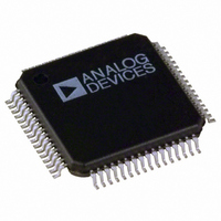
AD9248BSTZ-65 Analog Devices Inc, AD9248BSTZ-65 Datasheet - Page 7

AD9248BSTZ-65
Manufacturer Part Number
AD9248BSTZ-65
Description
IC ADC 14BIT DUAL 65MSPS 64-LQFP
Manufacturer
Analog Devices Inc
Specifications of AD9248BSTZ-65
Data Interface
Parallel
Number Of Bits
14
Sampling Rate (per Second)
65M
Number Of Converters
2
Power Dissipation (max)
600mW
Voltage Supply Source
Single Supply
Operating Temperature
-40°C ~ 85°C
Mounting Type
Surface Mount
Package / Case
64-LQFP
Resolution (bits)
14bit
Input Channel Type
Differential
Supply Voltage Range - Analogue
2.7V To 3.6V
Supply Voltage Range - Digital
2.25V To 3.6V
Supply Current
200mA
Sampling Rate
65MSPS
Rohs Compliant
Yes
Lead Free Status / RoHS Status
Lead free / RoHS Compliant
For Use With
AD9248BST-65EBZ - BOARD EVAL WITH AD9248BST-65AD9248BCP-65EBZ - BOARD EVAL WITH AD9248BCP-65
Lead Free Status / RoHS Status
Lead free / RoHS Compliant, Lead free / RoHS Compliant
Available stocks
Company
Part Number
Manufacturer
Quantity
Price
Company:
Part Number:
AD9248BSTZ-65
Manufacturer:
ADI
Quantity:
513
Company:
Part Number:
AD9248BSTZ-65
Manufacturer:
Analog Devices Inc
Quantity:
10 000
Part Number:
AD9248BSTZ-65
Manufacturer:
ADI/亚德诺
Quantity:
20 000
SWITCHING SPECIFICATIONS
AVDD = 3 V, DRVDD = 2.5 V, maximum sample rate, CLK_A = CLK_B; A
T
Table 4.
Parameter
SWITCHING PERFORMANCE
DATA OUTPUT PARAMETER
OUT-OF-RANGE RECOVERY TIME
1
2
3
The AD9248-65 model has a duty cycle stabilizer circuit that, when enabled, corrects for a wide range of duty cycles (see Figure 24).
Output delay is measured from clock 50% transition to data 50% transition, with a 5 pF load on each output.
Wake-up time is dependent on the value of the decoupling capacitors; typical values shown with 0.1 μF and 10 μF capacitors on REFT and REFB.
MIN
Maximum Conversion Rate
Minimum Conversion Rate
CLK Period
CLK Pulse-Width High
CLK Pulse-Width Low
Output Delay
Pipeline Delay (Latency)
Aperture Delay (t
Aperture Uncertainty (t
Wake-Up Time
to T
ANALOG
CLOCK
MAX
INPUT
DATA
OUT
, DCS enabled, unless otherwise noted.
2
3
(t
PD
A
)
)
1
N–9
1
J
N–1
)
N–8
N
Temp
Full
Full
Full
Full
Full
Full
Full
Full
Full
Full
Full
N–7
N+1
Test
Level
VI
V
V
V
V
VI
V
V
V
V
V
N–6
Min
50.0
15.0
15.0
2
20
N+2
AD9248BST/BCP-20
Figure 2. Timing Diagram
Rev. B | Page 7 of 48
N–5
Typ
3.5
7
1.0
0.5
2.5
2
N+3
Max
6
1
N–4
IN
N+4
= −0.5 dBFS differential input, 1.0 V internal reference,
Min
25.0
8.8
8.8
2
40
AD9248BST/BCP-40
N–3
N+5
Typ
3.5
7
1.0
0.5
2.5
2
N–2
N+6
Max
6
1
N–1
N+7
Min
65
15.4
6.2
6.2
2
AD9248BST/BCP-65
N
t
Typ
3.5
7
1.0
0.5
2.5
2
PD
N+8
=
MIN 2.0ns,
MAX 6.0ns
Max
1
6
AD9248
Unit
MSPS
MSPS
ns
ns
ns
ns
Cycles
ns
ps rms
ms
Cycles


