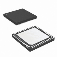
KAD5512P-21Q48 Intersil, KAD5512P-21Q48 Datasheet - Page 33

KAD5512P-21Q48
Manufacturer Part Number
KAD5512P-21Q48
Description
IC ADC 12BIT 210MSPS SGL 48-QFN
Manufacturer
Intersil
Series
FemtoCharge™r
Datasheet
1.KAD5512P-25Q72.pdf
(36 pages)
Specifications of KAD5512P-21Q48
Number Of Bits
12
Sampling Rate (per Second)
210M
Data Interface
Serial, SPI™
Number Of Converters
1
Power Dissipation (max)
271mW
Voltage Supply Source
Single Supply
Operating Temperature
-40°C ~ 85°C
Mounting Type
Surface Mount
Package / Case
48-VQFN
For Use With
KDC5512-Q48EVAL - DAUGHTER CARD FOR KAD5512KDC5512EVAL - DAUGHTER CARD FOR KAD5512
Lead Free Status / RoHS Status
Lead free / RoHS Compliant
Revision History
4/23/2009 FN6807.3 1) Added nap mode, sleep mode wake up times to spec table
12/23/08
08/19/09
7/30/08
12/5/08
2/25/09
DATE
REVISION
FN6807.0 Converted to intersil template. Assigned file number FN6807. Rev 0 - first release (as preliminary data
FN6807.1 P1; revised Key Specs
FN6807.2 Changed “odd” bits N in Figure 1A - DDR to “even” bits N, Replaced POD L48.7x7E due to changed
Rev 1
Initial Release of Production Data sheet
15) Updated Sinad 10MHz SINAD typical (170Msps)
sheet) with new file number.
P2; added Part Marking column to Order Info
P4; moved Thermal Resistance to Thermal Info table and added Theta JA Note 3 per packaging
P4-6; revisions throughout spec tables. Removed note from Elec Specs (Nap Mode must be invoked
using SPI.) Added notes 9 and 10 to Switching Specs.
P9; revised function for Pin 22 OUTMODE, Pin 23 NAPSLP and Pin 70 OUTFMT
P11; revised function for Pin 16 NAPSLP
P13-15; Performance curves revised throughout
P17; User Initiated Reset - revised 2nd sentence of 1st paragraph
P19; Nap/Sleep - revised 1st and 2nd sentences of 2nd paragraph
P23; Address 0x24: Gain_Fine; added 2 sentences to end of 1st paragraph.
Revised Table 8
P22; Serial Peripheral Interface- 1st paragraph; revised 2nd and 4th sentences.
P24; removed Figure (PHASE SLIP: CLK÷2 MODE, fCLOCK = 500MHz)
Address 0x71: Phase_slip; added sentence to end of paragraph
P27; revised Fig 45
P27; Table 16; revised Bits7:4, Addr C0
Throughout; formatted graphics to Intersil standards
dimension from “9.80 sq” to “6.80” sq. in land pattern
2) Added CSB, SCLK Setup time specs for nap, sleep modes
3) Added section showing 72pin/48pin package feature differences and default state for clkdiv, outmode,
outfmt page 27
4) Changed SPI setup time specs wording in spec table
5) Added ‘Reserved’ to SPI memory map at address 25H
6) Renumbered Notes
7) Added test platform link on page 31
8) Added ddr enable Note15 for 48 pin/72 pin options
9) Changed pin description table for 72/48 pin option, added DDR notes
10) Changed multi device note in spi physical interface section to show 3-wire application.page 24
11) Updated digital output section for ddr operation page 21
12) Change to fig 25 and fig 26 and description in text
13) Added connect note for thermal pad
14) Formatted Figures 25 and 26 with Intersil Standards
16) Updated sleep mode Power spec
17) Change to SPI interface section in spec table, timing in cycles now, added write, read specific timing
specs.
18) Updated SPI timing diagrams, Figures 37, 38
19) Updated wakeup time description in “Nap/Sleep” on page 21.
20) Removed calibration note in spec table
21) Updated fig 46 label)
22) Updated cal paragraph in user initiated reset section per DC.
33
KAD5512P
CHANGE
October 1, 2010
FN6807.4


