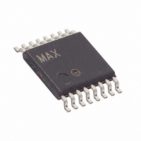
MAX1415EUE+T Maxim Integrated Products, MAX1415EUE+T Datasheet - Page 21

MAX1415EUE+T
Manufacturer Part Number
MAX1415EUE+T
Description
IC ADC 16BIT DELTA SIGMA 16TSSOP
Manufacturer
Maxim Integrated Products
Datasheet
1.MAX1415EUE.pdf
(36 pages)
Specifications of MAX1415EUE+T
Number Of Bits
16
Sampling Rate (per Second)
500
Data Interface
MICROWIRE™, QSPI™, Serial, SPI™
Number Of Converters
1
Power Dissipation (max)
755mW
Voltage Supply Source
Single Supply
Operating Temperature
-45°C ~ 85°C
Mounting Type
Surface Mount
Package / Case
16-TSSOP
Lead Free Status / RoHS Status
Lead free / RoHS Compliant
Table 5. Input Sampling Capacitor vs. Gain
Increasing the gain increases the resolution of the ADC
(LSB size decreases), but reduces the differential input
voltage range. Calculate 1 LSB in unipolar mode using
the following equation:
where: V
For a gain of 1 and V
in unipolar mode is 2.5V and 1 LSB ≈ 38.1µV. For a
gain of 4, the full-scale voltage in unipolar mode is
0.625V (V
input voltage range in this example reduces from 2.5V
to 0.625V, and the resolution increases since the LSB
size decreases from 38.1µV to 9.5µV.
Calculate 1 LSB in bipolar mode using the following
equation:
where: V
The B/U bit in the setup register
the MAX1415/MAX1416 for unipolar or bipolar transfer
functions. Figures 4 and 5 illustrate the unipolar and
bipolar transfer functions, respectively.
In unipolar mode, the digital output code is straight
binary. When AIN+ = AIN-, the outputs are at zero
scale, which is the lower endpoint of the transfer func-
tion. The full-scale endpoint is given by AIN+ - AIN- =
V
In bipolar mode, the digital output code is in offset
binary. Positive full scale is given by AIN+ - AIN- =
+V
AIN- = -V
are at zero scale, which is the midpoint of the bipolar
transfer function.
REF
REF
8–128
GAIN
/ GAIN, where V
1
2
4
/ GAIN and negative full scale is given by AIN+ -
REF
REF
REF
REF
= V
= V
/GAIN) and 1 LSB ≈ 9.5µV. The differential
/ GAIN. When AIN+ = AIN-, the outputs
1
REF+
REF+
INPUT SAMPLING CAPACITOR (C
LSB
1
______________________________________________________________________________________
LSB
Unipolar and Bipolar Modes
=
REF
- V
- V
REF
GAIN
=
REF-.
REF-.
GAIN
= V
= 2.5V, the full-scale voltage
V
REF
REF+
( ,
65 536
V
REF
( ,
65 536
(pF)
3.75
7.5
15
30
(Table 9) configures
- V
)
REF-
×
)
2
.
16-Bit, Low-Power, 2-Channel,
SAMP
)
When the MAX1415/MAX1416 are in buffered mode, the
absolute and common-mode analog input voltage
ranges reduce to between (GND + 50mV) and (V
1.5V). The differential input voltage range is not affected
in buffered mode.
Figure 4. MAX1415/MAX1416 Unipolar Transfer Function
Figure 5. MAX1415/MAX1416 Bipolar Transfer Function
1111 1111 1111 1111
1111 1111 1111 1110
1111 1111 1111 1101
1111 1111 1111 1100
0000 0000 0000 0011
0000 0000 0000 0010
0000 0000 0000 0001
0000 0000 0000 0000
1111 1111 1111 1111
1111 1111 1111 1110
1111 1111 1111 1101
1000 0000 0000 0001
1000 0000 0000 0000
0111 1111 1111 1111
0000 0000 0000 0010
0000 0000 0000 0001
0000 0000 0000 0000
Sigma-Delta ADCs
-32,768
0
1 LSB =
1
1 LSB =
-32,766
2
(GAIN) (65,536)
V
(GAIN) (65,536)
REF
3
/GAIN
V
REF
V
REF
DIFFERENTIAL INPUT VOLTAGE (LSB)
DIFFERENTIAL INPUT VOLTAGE (LSB)
-1
x 2
V
FULL-SCALE TRANSITION
REF
0
/GAIN
+1
V
REF
+32,765
/GAIN
65,533
+32,767
65,535
DD
21
-


