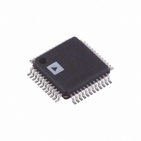
AD7664AST Analog Devices Inc, AD7664AST Datasheet

AD7664AST
Specifications of AD7664AST
Available stocks
Related parts for AD7664AST
AD7664AST Summary of contents
Page 1
FEATURES Throughput: 570 kSPS (Warp Mode) 500 kSPS (Normal Mode) 444 kSPS (Impulse Mode) INL: 2.5 LSB Max ( 0.0038% of Full Scale) 16-Bit Resolution with No Missing Codes S/(N+D Typ @ 45 kHz THD: –100 dB ...
Page 2
AD7664 –SPECIFICATIONS Parameter RESOLUTION ANALOG INPUT Voltage Range Operating Input Voltage Analog Input CMRR Input Current Input Impedance THROUGHPUT SPEED Complete Cycle Throughput Rate Time between Conversions Complete Cycle Throughput Rate Complete Cycle Throughput Rate DC ACCURACY Integral Linearity Error ...
Page 3
Parameter 8 TEMPERATURE RANGE Specified Performance NOTES LSB means least significant bit. With the 2.5 V input range, one LSB is 38.15 µ See Definition of Specifications section. These specifications do not include the error ...
Page 4
... Specification is for device in free air: 48-Lead LFCSP; θ = 26°C/W. JA Model AD7664AST AD7664ASTRL AD7664ACP AD7664ACPRL 1 EVAL-AD7664CB EVAL-CONTROL-BRD2 NOTES 1 This board can be used as a standalone evaluation board or in conjunction with the EVAL-CONTROL-BRD2 for evaluation/ demonstration purposes. 2 This board allows control and communicate with all Analog Devices evaluation boards ending in the CB designators. ...
Page 5
CONNECT Pin No. Mnemonic Type Description 1 AGND P Analog Power Ground Pin. 2 AVDD P Input Analog Power Pins. Nominally 40–42 Connect. 44–48 4 DGND DI Must Be Tied to the ...
Page 6
AD7664 Pin No. Mnemonic Type 16 D7 DI/O or RDC/SDIN 17 OGND P 18 OVDD P 19 DVDD P 20 DGND SDOUT 22 D9 DI/O or SCLK 23 D10 DO or SYNC 24 D11 DO ...
Page 7
Pin No. Mnemonic Type CNVST AGND P 37 REF AI 38 REFGND AI 39 INGND NOTES AI = Analog Input DI = Digital Input DI/O = Bidirectional Digital DO = Digital Output P ...
Page 8
Performance Characteristics AD7664 2.5 2.0 1.5 1.0 0.5 0 –0.5 –1.0 –1.5 –2.0 –2.5 0 16384 32768 CODE TPC 1. Integral Nonlinearity vs. Code 8000 7288 7148 7000 6000 5000 4000 3000 2000 753 1000 ...
Page 9
POINT FFT – 570kHz 45.5322kHz, –0.5dB IN –40 SNR = 90.1dB SINAD = 89.4dB THD = –97.1dB –60 SFDR = 97.5dB –80 –100 –120 –140 –160 –180 0 57 114 171 FREQUENCY (kHz) ...
Page 10
AD7664 10 8 FULL-SCALE ERROR –2 –4 –6 –8 –10 –55 –35 – TEMPERATURE ( C) TPC 13. Zero Error, Full-Scale Error vs. Temperature 50 OVDD = 2.7V ...
Page 11
CIRCUIT INFORMATION The AD7664 is a very fast, low power, single-supply, precise 16-bit analog-to-digital converter (ADC). The AD7664 features different modes to optimize performances according to the applications. In Warp Mode, the AD7664 is capable of converting 570,000 samples per ...
Page 12
AD7664 The Normal Mode is the fastest mode (500 kSPS) without any limitation on the time between conversions. This mode makes the AD7664 ideal for asynchronous applications such as data acquisition systems, where both high accuracy and fast sample rate ...
Page 13
Analog Input Figure 6 shows an equivalent circuit of the input structure of the AD7664. AVDD INGND C1 D2 AGND Figure 6. Equivalent Analog Input Circuit The two diodes D1 and D2 provide ESD protection for the ...
Page 14
AD7664 For instance driver like the AD8021, with an equivalent input noise of 2 nV/√Hz and configured as a buffer, thus with a noise gain of 1, the SNR degrades by 0.58 dB. • The driver needs to ...
Page 15
CONVERSION CONTROL Figure 11 shows the detailed timing diagrams of the conversion process. The AD7664 is controlled by the signal CNVST, which initiates conversion. Once initiated, it cannot be restarted or aborted, even by the power-down input PD, until the ...
Page 16
AD7664 CNVST, RD BUSY t 3 PREVIOUS DATABUS CONVERSION Figure 15. Slave Parallel Data Timing for Reading (Read during Convert) CS CNVST BUSY t 29 SYNC t 14 ...
Page 17
CS BUSY SCLK t 31 SDOUT t 16 SDIN t 33 Figure 18. Slave Serial Data Timing for Reading (Read after Convert) Because the AD7664 is used with a fast throughput, the Mas- ter Read During Conversion Mode is the ...
Page 18
AD7664 CS CNVST BUSY t 3 SCLK t 31 SDOUT t 16 Figure 20. Slave Serial Data Timing for Reading (Read Previous Conversion during Convert) External Clock Data Read during Conversion Figure 20 shows the detailed timing diagram of this ...
Page 19
APPLICATION HINTS Bipolar and Wider Input Ranges In some applications desired to use a bipolar or wider ana- log input range like, for instance, ± ± Although the ...
Page 20
AD7664 1.45 1.40 1.35 0.15 SEATING 0.05 PLANE ROTATED 90 CCW 7.00 BSC SQ PIN 1 INDICATOR TOP VIEW 1.00 12 MAX 0.85 0.80 SEATING PLANE OUTLINE DIMENSIONS 48-Lead Low Profile Quad Flat Package [LQFP] (ST-48) Dimensions shown in millimeters ...
Page 21
Revision History Location 1/04—Data Sheet changed from REV REV. E. Changes to title . . . . . . . . . . . . . . . . . . . . . . . . . ...
Page 22
AD7664 Revision History Location 8/01—Data Sheet changed from REV REV. B. Edit to FEATURES . . . . . . . . . . . . . . . . . . . . . . . . ...
Page 23
–23– ...
Page 24
–24– ...


