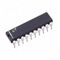
LTC1289CCN Linear Technology, LTC1289CCN Datasheet - Page 14

LTC1289CCN
Manufacturer Part Number
LTC1289CCN
Description
IC DATA ACQ SYS 12BIT 3V 20-DIP
Manufacturer
Linear Technology
Type
Data Acquisition System (DAS)r
Datasheet
1.LTC1289CCN.pdf
(28 pages)
Specifications of LTC1289CCN
Resolution (bits)
12 b
Sampling Rate (per Second)
25k
Data Interface
Serial, Parallel
Voltage Supply Source
Dual ±
Voltage - Supply
3V
Operating Temperature
0°C ~ 70°C
Mounting Type
Through Hole
Package / Case
20-DIP (0.300", 7.62mm)
Lead Free Status / RoHS Status
Contains lead / RoHS non-compliant
Available stocks
Company
Part Number
Manufacturer
Quantity
Price
Company:
Part Number:
LTC1289CCN
Manufacturer:
Epson
Quantity:
6 029
LTC1289
Deglitcher
A deglitching circuit has been added to the Chip Select
input of the LTC1289 to minimize the effects of errors
caused by noise on that input. This circuit ignores changes
in state on the CS input that are shorter in duration than
one ACLK cycle. After a change of state on the CS input, the
LTC1289 waits for two falling edge of the ACLK before
recognizing a valid chip select. One indication of CS
recognition is the D
Hi-Z state). Note that the deglitching applies to both the
rising and falling CS edges.
14
A
ACLK
D
OUT
PPLICATI
CS
SCLK
SCLK
D
D
OUT
OUT
D
D
CS
CS
IN
IN
B11 B10 B9
B11 B10 B9
MUX ADDRESS
MUX ADDRESS
Low CS Recognized Internally
Hi-Z
O
SHIFT
SHIFT
IN
IN
OUT
U
S
line becoming active (leaving the
B8
B8
I FOR ATIO
U
B7
B7
B6
B6
B5
B5
SAMPLE ANALOG
SAMPLE ANALOG
W
VALID OUTPUT
B4
B4
INPUT
INPUT
t
t
SMPL
SMPL
B3
B3
Figure 3. CS High During Conversion
Figure 4. CS Low During Conversion
B2
B2
DON'T CARE
DON'T CARE
B1
U
B1
LTC1289 AI08
B0
B0
REMAIN LOW
ACLK CYC
ACLK CYC
SCLK MUST
48 TO 52
48 TO 52
CS Low During Conversion
In the normal mode of operation, CS is brought high
during the conversion time. The serial port ignores any
SCLK activity while CS is high. The LTC1289 will also
operate with CS low during the conversion. In this mode,
SCLK must remain low during the conversion as shown in
the following figure. After the conversion is complete, the
D
the data transfer can begin as normal.
ACLK
D
OUT
OUT
CS
B11 B10 B9
line will become active with the first output bit. Then
B11 B10 B9 B8
VALID OUTPUT
High CS Recognized Internally
B8
AND NEW ADDRESS IN
AND NEW ADDRESS IN
SHIFT RESULT OUT
SHIFT RESULT OUT
B7
B7
B6
B6
B5
B5
B4
B4
B3
B3
B2
B2
Hi-Z
B1
B1 B0
B0
LTC1289 AIF04
LTC1289 AIF03
LTC1289 AI08a
1289fb


