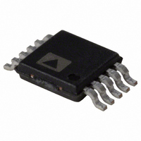
AD5259BRMZ100 Analog Devices Inc, AD5259BRMZ100 Datasheet - Page 14

AD5259BRMZ100
Manufacturer Part Number
AD5259BRMZ100
Description
IC DGTL POT 100K 256POS 10-MSOP
Manufacturer
Analog Devices Inc
Datasheet
1.AD5259BRMZ10.pdf
(24 pages)
Specifications of AD5259BRMZ100
Taps
256
Resistance (ohms)
100K
Number Of Circuits
1
Temperature Coefficient
500 ppm/°C Typical
Memory Type
Non-Volatile
Interface
I²C, 2-Wire Serial
Voltage - Supply
2.7 V ~ 3.3 V, 4.5 V ~ 5.5 V
Operating Temperature
-40°C ~ 85°C
Mounting Type
Surface Mount
Package / Case
10-MSOP, Micro10™, 10-uMAX, 10-uSOP
Resistance In Ohms
100K
End To End Resistance
100kohm
Track Taper
Linear
Resistance Tolerance
± 30%
No. Of Steps
256
Supply Voltage Range
2.7V To 5.5V
Control Interface
I2C, Serial
No. Of Pots
Single
Lead Free Status / RoHS Status
Lead free / RoHS Compliant
For Use With
AD5259EVAL - BOARD EVAL FOR AD5259 DGTL POT
Lead Free Status / RoHS Status
Lead free / RoHS Compliant, Lead free / RoHS Compliant
Available stocks
Company
Part Number
Manufacturer
Quantity
Price
Part Number:
AD5259BRMZ100
Manufacturer:
ADI/亚德诺
Quantity:
20 000
Part Number:
AD5259BRMZ100-R7
Manufacturer:
ADI/亚德诺
Quantity:
20 000
AD5259
THEORY OF OPERATION
The AD5259 is a 256-position digitally-controlled variable
resistor (VR) device. EEPROM is pre-loaded at midscale from
the factory, and initial power-up is, accordingly, at midscale.
PROGRAMMING THE VARIABLE RESISTOR
Rheostat Operation
The nominal resistance (R
and Terminal B is available in 5 kΩ, 10 kΩ, 50 kΩ, and 100 kΩ.
The nominal resistance of the VR has 256 contact points accessed
by the wiper terminal. The 8-bit data in the RDAC latch is
decoded to select one of 256 possible settings.
The general equation determining the digitally programmed
output resistance between Wiper W and Terminal B is
where:
D is the decimal equivalent of the binary code loaded in the
8-bit RDAC register.
R
R
each internal switch.
In the zero-scale condition, there is a relatively low value finite
wiper resistance. Care should be taken to limit the current flow
between Wiper W and Terminal B in this state to a maximum
pulse current of no more than 20 mA. Otherwise, degradation
or destruction of the internal switch contact can occur.
AB
W
is the wiper resistance contributed by the ON resistance of
is the end-to-end resistance.
R
WB
(
D
A
B
)
Figure 39. AD5259 Equivalent RDAC Circuit
Figure 38. Rheostat Mode Configuration
256
D7
D6
D5
D4
D3
D2
D1
D0
DECODER
D
W
LATCH
RDAC
AND
R
AB
AB
A
B
) of the RDAC between Terminal A
2
R
R
R
R
S
S
S
S
R
W
W
A
B
A
W
B
W
Rev. B | Page 14 of 24
(1)
Similar to the mechanical potentiometer, the resistance of the
RDAC between Wiper W and Terminal A produces a digitally
controlled complementary resistance, R
setting for R
decreases as the data loaded in the latch increases in value.
The general equation for this operation is
Typical device-to-device matching is process lot dependent and
may vary by up to ±30%. For this reason, resistance tolerance is
stored in the EEPROM, enabling the user to know the actual
R
PROGRAMMING THE POTENTIOMETER DIVIDER
Voltage Output Operation
The digital potentiometer easily generates a voltage divider at
Wiper W to Terminal B and Wiper W to Terminal A propor-
tional to the input voltage at Terminal A to Terminal B. Unlike
the polarity of V
across Terminal A to Terminal B, Wiper W to Terminal A, and
Wiper W to Terminal B can be at either polarity.
If ignoring the effect of the wiper resistance for approximation,
connecting the A terminal to 5 V and the B terminal to ground
produces an output voltage at Wiper W to Terminal B starting
at 0 V up to 1 LSB less than 5 V. The general equation defining
the output voltage at V
input voltage applied to Terminal A and Terminal B is
A more accurate calculation, which includes the effect of wiper
resistance, V
Operation of the digital potentiometer in the divider mode
results in a more accurate operation over temperature. Unlike
the rheostat mode, the output voltage is dependent mainly
on the ratio of the Internal Resistors R
the absolute values.
AB
within 0.1%.
V
V
R
WA
W
W
(
(
D
D
(
D
)
)
)
WA
W
Figure 40. Potentiometer Mode Configuration
, is
256
R
starts at a maximum value of resistance and
D
256
WB
DD
R
256
AB
V
(
to GND, which must be positive, voltage
D
A
)
D
W
V
V
I
256
A
with respect to ground for any valid
R
256
AB
R
WA
A
B
D
R
AB
2
V
(
D
W
B
)
R
V
W
B
WA
V
WA
O
and R
. The resistance value
WB
and not
(2)
(3)
(4)


