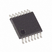
MAX5482EUD+ Maxim Integrated Products, MAX5482EUD+ Datasheet - Page 14

MAX5482EUD+
Manufacturer Part Number
MAX5482EUD+
Description
IC DGTL POT 10BIT NV 14-TSSOP
Manufacturer
Maxim Integrated Products
Datasheet
1.MAX5481EUD.pdf
(20 pages)
Specifications of MAX5482EUD+
Taps
1024
Resistance (ohms)
50K
Number Of Circuits
1
Temperature Coefficient
35 ppm/°C Typical
Memory Type
Non-Volatile
Interface
SPI, 3-Wire Serial
Voltage - Supply
2.7 V ~ 5.25 V, ±2.5 V ~ 5.25 V
Operating Temperature
-40°C ~ 85°C
Mounting Type
Surface Mount
Package / Case
14-TSSOP
Resistance In Ohms
50K
Number Of Pots
Single
Taps Per Pot
1024
Resistance
50 KOhms
Wiper Memory
Non Volatile
Digital Interface
Serial (3-Wire, SPI)
Operating Supply Voltage
2.7 V to 5.25 V
Supply Current
1 uA
Maximum Operating Temperature
+ 85 C
Minimum Operating Temperature
- 40 C
Description/function
1024-Tap 50k Nonvolatile Linear-Taper Digital Potentiometer (Voltage Divider)
Mounting Style
SMD/SMT
Supply Voltage (max)
5.25 V
Supply Voltage (min)
2.7 V
Tolerance
25 %
Lead Free Status / RoHS Status
Lead free / RoHS Compliant
Drive SPI/UD high to enable the 3-wire SPI-compatible
serial interface (see Figure 3). This write-only interface
contains three inputs: chip select (CS), data in
(DIN(U/D)), and data clock (SCLK(INC)). Drive CS low
to load the data at DIN(U/D) synchronously into the shift
register on each SCLK(INC) rising edge.
The WRITE command (C1, C0 = 00) requires 24 clock
cycles to transfer the command and data (Figure 4a).
The COPY commands (C1, C0 = 10 or 11) use either
eight clock cycles to transfer the command bits (Figure
4b) or 24 clock cycles with the last 16 data bits disre-
garded by the device.
After loading the data into the shift register, drive CS
high to latch the data into the appropriate control regis-
ter. Keep CS low during the entire serial data stream to
avoid corruption of the data. Table 2 shows the com-
mand decoding.
10-Bit, Nonvolatile, Linear-Taper Digital
Potentiometers
Table 2. Command Decoding*
* D9 is the MSB and D0 is the LSB.
X = Don’t care.
Figure 3. SPI-Compatible Serial-Interface Timing Diagram (SPI/UD = 1)
14
CLOCK EDGE
Bit Name
Write Wiper Register
Copy Wiper Register
to NV Register
Copy NV Register to
Wiper Register
______________________________________________________________________________________
SCLK(INC)
DIN(U/D)
SPI-Compatible Serial Interface
CS
—
1
0
0
0
t
CSO
—
2
0
0
0
C1
3
0
1
1
t
CSS
C0
4
0
0
1
t
DS
—
5
0
0
0
—
6
0
0
0
t
CL
—
7
0
0
0
t
DH
—
t
8
0
0
0
CH
D9
D9
—
—
9
Data written to this register (C1, C0 = 00) controls the
wiper position. The 10 data bits (D9–D0) indicate the
position of the wiper. For example, if DIN(U/D) = 00 0000
0000, the wiper moves to the position closest to L. If
DIN(U/D) = 11 1111 1111, the wiper moves closest to H.
This command writes data to the volatile random
access memory (RAM), leaving the NV register
unchanged. When the device powers up, the data
stored in the NV register transfers to the wiper register,
moving the wiper to the stored position. Figure 5 shows
how to write data to the wiper register.
D8
D8
10
—
—
D7
D7
11
—
—
D6
D6
12
—
—
t
CP
D5
D5
13
—
—
D4
D4
14
—
—
t
D3
D3
CSH
15
—
—
D2
D2
16
—
—
t
CS1
Write Wiper Register
D1
D1
17
—
—
t
CSW
D0
D0
18
—
—
19
—
—
—
X
…
…
…
…
…
24
—
—
—
X


