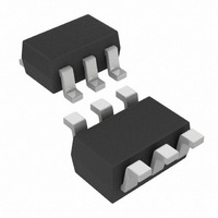
MCP4017T-103E/LT Microchip Technology, MCP4017T-103E/LT Datasheet - Page 44

MCP4017T-103E/LT
Manufacturer Part Number
MCP4017T-103E/LT
Description
IC DGTL POT 10K 128TAPS SC70-6
Manufacturer
Microchip Technology
Datasheet
1.MCP4018T-502ELT.pdf
(66 pages)
Specifications of MCP4017T-103E/LT
Package / Case
SC-70-6, SC-88, SOT-363
Temperature Coefficient
150 ppm/°C Typical
Taps
128
Resistance (ohms)
10K
Number Of Circuits
1
Memory Type
Volatile
Interface
I²C, 2-Wire Serial
Voltage - Supply
1.8 V ~ 5.5 V
Operating Temperature
-40°C ~ 125°C
Mounting Type
Surface Mount
Resistance In Ohms
10K
Number Of Pots
Single
Taps Per Pot
128
Resistance
10 KOhms
Wiper Memory
Volatile
Buffered Wiper
Buffered
Digital Interface
Serial (2-Wire, I2C)
Operating Supply Voltage
2.5 V or 3.3 V or 5 V
Supply Current
0.045 mA (Typ)
Maximum Operating Temperature
+ 125 C
Minimum Operating Temperature
- 40 C
Description/function
7 Bit Single I2C Digital Rheostat
Mounting Style
SMD/SMT
Supply Voltage (max)
5.5 V
Supply Voltage (min)
1.8 V
Tolerance
20 %
Lead Free Status / RoHS Status
Lead free / RoHS Compliant
Lead Free Status / RoHS Status
Lead free / RoHS Compliant, Lead free / RoHS Compliant
Other names
MCP4017T-103E/LTTR
Available stocks
Company
Part Number
Manufacturer
Quantity
Price
Part Number:
MCP4017T-103E/LT
Manufacturer:
MICROCHIP/微芯
Quantity:
20 000
MCP4017/18/19
6.3
Wiper resistance is the series resistance of the analog
switch that connects the selected resistor ladder node
to the Wiper Terminal common signal (see
A value in the volatile wiper register selects which
analog switch to close, connecting the W terminal to
the selected node of the resistor ladder.
The resistance is dependent on the voltages on the
analog switch source, gate, and drain nodes, as well as
the device’s wiper code, temperature, and the current
through the switch. As the device voltage decreases,
the wiper resistance increases (see
Table
The wiper can connect directly to Terminal B or to
Terminal A. A zero scale connections, connects the
Terminal W (wiper) to Terminal B (wiper setting of
000h). A full scale connections, connects the Terminal
W (wiper) to Terminal A (wiper setting of 7Fh). In these
configurations the only resistance between the
Terminal W and the other Terminal (A or B) is that of the
analog switches.
The wiper resistance is typically measured when the
wiper is positioned at either zero scale (00h) or full
scale (3Fh).
The wiper resistance in potentiometer-generated
voltage divider applications is not a significant source
of error.
The wiper resistance in rheostat applications can
create significant nonlinearity as the wiper is moved
toward zero scale (00h). The lower the nominal
resistance, the greater the possible error.
In a rheostat configuration, this change in voltage
needs to be taken into account. Particularly for the
lower resistance devices. For the 5.0 kΩ device the
maximum wiper resistance at 5.5V is approximately
3.2% of the total resistance, while at 2.7V it is
approximately 6.5% of the total resistance.
TABLE 6-4:
DS22147A-page 44
5000
10000
50000
100000
Note 1:
(R
Total
AB
6-4).
Typical
)
2:
Wiper Resistance
393.70
787.40
R
R
39.37
78.74
Step
(R
S
AB
S
is the typical value. The variation of this resistance is minimal over voltage.
Resistance (Ω)
)
is the typical value. The variation of this resistance is minimal over voltage.
TYPICAL STEP RESISTANCES AND RELATIONSHIP TO WIPER RESISTANCE
Typical
100
100
100
100
Wiper (R
Max @
5.5V
170
170
170
170
W
)
Figure 6-4
Max @
2.7V
325
325
325
325
Figure
254.00%
127.00%
6-1).
Typical
25.40%
12.70%
and
R
W
=
R
W
R
431.80%
215.90%
43.18%
21.59%
@ 5.5V
/ R
W
In a potentiometer configuration, the wiper resistance
variation does not effect the output voltage seen on the
W pin.
The slope of the resistance has a linear area (at the
higher voltages) and a non-linear area (at the lower
voltages). In where resistance increases faster then the
voltage drop (at low voltages).
FIGURE 6-4:
Resistance (R
Since there is minimal variation of the total device
resistance over voltage, at a constant temperature (see
Figure
the change in wiper resistance over voltage can have a
significant impact on the INL and DNL error.
= Max
S
Note: The slope of the resistance has a linear
R
(%)
W
(1)
2-11,
R
area (at the higher voltages) and a
non-linear area (at the lower voltages).
412.75%
825.5%
82.55%
@ 2.7V
41.28%
W
= Max
Figure
W
) to Voltage.
2-29,
Typical
2.00%
1.00%
0.20%
0.10%
Relationship of Wiper
R
© 2009 Microchip Technology Inc.
W
Figure
V
=
DD
R
W
R
/ R
2-47, or
@ 5.5V
W
3.40%
1.70%
0.34%
0.17%
AB
= Max
(%)
Figure
(2)
R
0.325%
@ 2.7V
W
6.50%
3.25%
0.65%
= Max
2-65),


