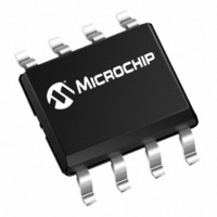
MCP4821-E/MS Microchip Technology, MCP4821-E/MS Datasheet - Page 18

MCP4821-E/MS
Manufacturer Part Number
MCP4821-E/MS
Description
IC DAC 12BIT W/SPI 8MSOP
Manufacturer
Microchip Technology
Datasheet
1.MCP4821-EMS.pdf
(48 pages)
Specifications of MCP4821-E/MS
Data Interface
Serial, SPI™
Settling Time
4.5µs
Number Of Bits
12
Number Of Converters
1
Voltage Supply Source
Single Supply
Operating Temperature
-40°C ~ 125°C
Mounting Type
Surface Mount
Package / Case
8-MSOP, Micro8™, 8-uMAX, 8-uSOP,
Resolution (bits)
12bit
Input Channel Type
Serial
Supply Voltage Range - Analog
2.7V To 5.5V
Supply Current
350µA
Digital Ic Case Style
MSOP
No. Of Pins
8
Lead Free Status / RoHS Status
Lead free / RoHS Compliant
Power Dissipation (max)
-
Lead Free Status / RoHS Status
Lead free / RoHS Compliant, Lead free / RoHS Compliant
Available stocks
Company
Part Number
Manufacturer
Quantity
Price
Company:
Part Number:
MCP4821-E/MS
Manufacturer:
Maxim
Quantity:
252
Part Number:
MCP4821-E/MS
Manufacturer:
MICROCHIP/微芯
Quantity:
20 000
MCP4801/4811/4821
4.0.2
A Differential Non-Linearity (DNL) error is the measure
of the variations in code widths from the ideal code
width. A DNL error of zero indicates that every code is
exactly 1 LSb wide.
FIGURE 4-2:
4.0.3
Offset error is the deviation from zero voltage output
when the digital input code is zero.
4.0.4
Gain error is the deviation from the ideal output,
V
DS22244B-page 18
REF
Digital
Input
Code
– 1 LSb, excluding the effects of offset error.
111
110
101
100
011
010
001
000
DNL ACCURACY
OFFSET ERROR
GAIN ERROR
Actual
Transfer
Function
DAC Output
Example for DNL Error.
Narrow Code, <1 LSb
Wide Code, >1 LSb
Ideal Transfer
Function
4.1
4.1.1
The analog DAC output is buffered with a low-power,
precision CMOS amplifier. This amplifier provides low
offset voltage and low noise. The output stage enables
the device to operate with output voltages close to the
power supply rails. Refer to Section 1.0 “Electrical
Characteristics” for the analog output voltage range
and load conditions.
In addition to resistive load-driving capability, the
amplifier will also drive high capacitive loads without
oscillation. The amplifier’s strong output allows V
be used as a programmable voltage reference in a
system.
4.1.1.1
The rail-to-rail output amplifier has two configurable
gain options: a gain of 1x (<GA> = 1) or a gain of 2x
(<GA> = 0). The default setting is a gain of 2x. This
results in an ideal full-scale output of 0.000V to 4.096V
due to the internal reference (V
4.1.2
The MCP4801/4811/4821 devices utilize internal
2.048V voltage reference. The voltage reference has a
low
characteristics. Refer to Section 1.0 “Electrical Char-
acteristics” for the voltage reference specifications.
temperature
Circuit Descriptions
OUTPUT AMPLIFIER
VOLTAGE REFERENCE
Programmable Gain Block
coefficient
2010 Microchip Technology Inc.
REF
= 2.048V).
and
low
OUT
noise
to


