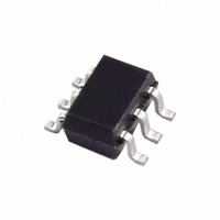
AD5611BKSZ-REEL7 Analog Devices Inc, AD5611BKSZ-REEL7 Datasheet - Page 17

AD5611BKSZ-REEL7
Manufacturer Part Number
AD5611BKSZ-REEL7
Description
IC DAC 10BIT SGL 2.7-5.5V SC70-6
Manufacturer
Analog Devices Inc
Series
nanoDAC™r
Datasheet
1.AD5601BKSZ-REEL7.pdf
(20 pages)
Specifications of AD5611BKSZ-REEL7
Settling Time
6µs
Number Of Bits
10
Data Interface
SPI™
Number Of Converters
1
Voltage Supply Source
Single Supply
Power Dissipation (max)
500µW
Operating Temperature
-40°C ~ 125°C
Mounting Type
Surface Mount
Package / Case
SC-70-6, SC-88, SOT-363
Lead Free Status / RoHS Status
Lead free / RoHS Compliant
Other names
AD5611BKSZ-REEL7TR
Available stocks
Company
Part Number
Manufacturer
Quantity
Price
Company:
Part Number:
AD5611BKSZ-REEL7
Manufacturer:
VISHAY
Quantity:
5 015
AD5601/AD5611/AD5621 to Blackfin® ADSP-BF53x
Interface
Figure 47 shows a serial interface between the AD5601/AD5611/
AD5621 and the Blackfin ADSP-BF53x microprocessor. The
ADSP-BF53x processor family incorporates two dual-channel
synchronous serial ports, SPORT1 and SPORT0, for serial and
multiprocessor communications. Using SPORT0 to connect to
the AD5601/AD5611/AD5621, the setup for the interface is as
follows: DT0PRI drives the SDIN pin of the AD5601/AD5611/
AD5621, while TSCLK0 drives the SCLK of the part. The SYNC
is driven from TFS0.
AD5601/AD5611/AD5621 to 80C51/80L51 Interface
Figure 48 shows a serial interface between the AD5601/
AD5611/AD5621 and the 80C51/80L51 microcontroller. The
setup for the interface is as follows: TxD of the 80C51/80L51
drives SCLK of the AD5601/AD5611/AD5621, while RxD
drives the serial data line of the part. The SYNC signal is again
derived from a bit programmable pin on the port. In this case,
Port Line P3.3 is used. When data is to be transmitted to the
AD5601/AD5611/AD5621, P3.3 is taken low. The 80C51/80L51
transmit data only in 8-bit bytes; therefore, only eight falling
clock edges occur in the transmit cycle. To load data to the
DAC, P3.3 is left low after the first eight bits are transmitted,
*ADDITIONAL PINS OMITTED FOR CLARITY
Figure 47. AD5601/AD5611/AD5621 to Blackfin ADSP-BF53x Interface
ADSP-BF53x*
TSCLK0
DT0PRI
TFS0
AD5601/AD5611/
AD5621*
SDIN
SCLK
SYNC
Rev. E | Page 17 of 20
and a second write cycle is initiated to transmit the second byte
of data. P3.3 is taken high following the completion of this
cycle. The 80C51/80L51 output the serial data LSB first. The
AD5601/AD5611/AD5621 require data with the MSB as the
first bit received. The 80C51/80L51 transmit routine should
take this into account.
AD5601/AD5611/AD5621 to MICROWIRE Interface
Figure 49 shows an interface between the AD5601/AD5611/
AD5621 and any MICROWIRE-compatible device. Serial data
is shifted out on the falling edge of the serial clock and is
clocked into the AD5601/AD5611/AD5621 on the rising edge
of the SK.
*ADDITIONAL PINS OMITTED FOR CLARITY
*ADDITIONAL PINS OMITTED FOR CLARITY
Figure 48. AD5601/AD5611/AD5621 to 80C51/80L51 Interface
Figure 49. AD5601/AD5611/AD5621 to MICROWIRE Interface
80C51/80L51*
MICROWIRE*
P3.3
RxD
TxD
SO
CS
SK
AD5601/AD5611/AD5621
AD5601/AD5611/
AD5621*
SYNC
SCLK
SDIN
AD5601/AD5611/
AD5621*
SYNC
SCLK
SDIN


