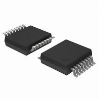
UDA1330ATS/N2,118 NXP Semiconductors, UDA1330ATS/N2,118 Datasheet - Page 6

UDA1330ATS/N2,118
Manufacturer Part Number
UDA1330ATS/N2,118
Description
IC STEREO FILTER DAC 16SSOP
Manufacturer
NXP Semiconductors
Datasheet
1.UDA1330ATSN2118.pdf
(23 pages)
Specifications of UDA1330ATS/N2,118
Package / Case
16-SSOP
Number Of Bits
20
Data Interface
Serial
Number Of Converters
2
Voltage Supply Source
Analog and Digital
Power Dissipation (max)
75mW
Operating Temperature
-40°C ~ 85°C
Mounting Type
Surface Mount
Conversion Rate
55 KSPS
Interface Type
Serial (3-Wire)
Operating Supply Voltage
5 V
Operating Temperature Range
+ 85 C
Mounting Style
SMD/SMT
Number Of Dac Outputs
2
Snr
100 dB (Typ)
Lead Free Status / RoHS Status
Lead free / RoHS Compliant
Settling Time
-
Lead Free Status / Rohs Status
Lead free / RoHS Compliant
Other names
935262880118
UDA1330ATSDK-T
UDA1330ATSDK-T
UDA1330ATSDK-T
UDA1330ATSDK-T
NXP Semiconductors
Interpolation filter (DAC)
The digital filter interpolates from 1f
a recursive filter and an FIR filter (see Table 4).
Table 4 Interpolation filter characteristics
Noise shaper
The 3rd-order noise shaper operates at 128f
in-band quantization noise to frequencies well above the
audio band. This noise shaping technique enables high
signal-to-noise ratios to be achieved. The noise shaper
output is converted into an analog signal using a Filter
Stream DAC (FSDAC).
2001 Feb 02
Pass-band ripple
Stop band
Dynamic range
Low-cost stereo filter DAC
ITEM
CONDITION
0 to 0.45f
0 to 0.45f
>0.55f
s
s
s
s
to 128f
VALUE (dB)
s
by cascading
s
. It shifts
±0.1
−50
108
6
Filter stream DAC
The FSDAC is a semi-digital reconstruction filter that
converts the 1-bit data stream of the noise shaper to an
analog output voltage. The filter coefficients are
implemented as current sources and are summed at virtual
ground of the output operational amplifier. In this way very
high signal-to-noise performance and low clock jitter
sensitivity is achieved. A post-filter is not needed due to
the inherent filter function of the DAC. On-board amplifiers
convert the FSDAC output current to an output voltage
signal capable of driving a line output.
The output voltage of the FSDAC scales linearly with the
power supply voltage.
Pin compatibility
In the L3 mode the UDA1330ATS can be used on boards
that are designed for the UDA1320ATS.
Remark: It should be noted that the UDA1330ATS is
designed for 5 V operation while the UDA1320ATS is
designed for 3 V operation. This means that the
UDA1330ATS can be used with the UDA1320ATS supply
voltage range, but the UDA1320ATS can not be used with
the 5 V supply voltage.
UDA1330ATS
Product specification


