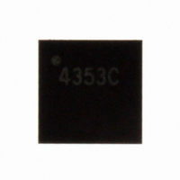
CS4353-CNZ Cirrus Logic Inc, CS4353-CNZ Datasheet - Page 17

CS4353-CNZ
Manufacturer Part Number
CS4353-CNZ
Description
IC DAC STER 106DB 2VRMS 24QFN
Manufacturer
Cirrus Logic Inc
Datasheet
1.CS4353-CNZ.pdf
(26 pages)
Specifications of CS4353-CNZ
Number Of Converters
1
Package / Case
24-QFN
Number Of Bits
24
Data Interface
Serial
Voltage Supply Source
Single Supply
Power Dissipation (max)
152mW
Operating Temperature
-40°C ~ 85°C
Mounting Type
Surface Mount
Number Of Dac Outputs
2
Resolution
24 bit
Interface Type
Serial
Supply Voltage (max)
3.47 V
Supply Voltage (min)
3.13 V
Maximum Operating Temperature
+ 125 C
Mounting Style
SMD/SMT
Maximum Power Dissipation
152 mW
Minimum Operating Temperature
- 55 C
Supply Current
10 mA
Lead Free Status / RoHS Status
Lead free / RoHS Compliant
For Use With
598-1519 - BOARD EVAL FOR CS4353 DAC
Settling Time
-
Lead Free Status / Rohs Status
Lead free / RoHS Compliant
Other names
598-1640
Available stocks
Company
Part Number
Manufacturer
Quantity
Price
Company:
Part Number:
CS4353-CNZ
Manufacturer:
CIRRUS
Quantity:
4 588
Part Number:
CS4353-CNZ
Manufacturer:
CIRRUS
Quantity:
20 000
Company:
Part Number:
CS4353-CNZR
Manufacturer:
TI
Quantity:
600
Part Number:
CS4353-CNZR
Manufacturer:
CIRRUS
Quantity:
20 000
CS4353
4.8
Initialization
When power is first applied, the DAC enters a reset (low power) state at the beginning of the initialization
sequence. In this state, the AOUTx pins are weakly pulled to ground and VBIAS is connected to VA.
The device will remain in the reset state until the RESET pin is brought high. Once the RESET pin is high,
the internal digital circuitry is reset and the DAC enters a power-down state until MCLK is applied. Alterna-
tively, if no external reset control is required, the internal power-on reset can be used by tying the RESET
pin to VL (see
Section
4.7).
Once MCLK is valid, the device enters an initialization state in which the charge pump powers up and charg-
es the capacitors for both the positive and negative high-voltage supplies.
Once LRCK and SCLK are valid, the number of MCLK cycles is counted relative to the LRCK period to de-
termine the MCLK/LRCK frequency ratio. Next, the device enters the power-up state in which the interpo-
lation and decimation filters and delta-sigma modulators are turned on, the internal voltage reference,
VBIAS, powers up to normal operation, the analog output pull-down resistors are removed, and power is
applied to the output amplifiers.
After this power-up state sequence is complete, normal operation begins and analog output is generated.
If valid MCLK, LRCK, and SCLK are applied to the DAC before RESET is set high, the total time from RE-
SET being set high to the analog audio output from AOUTx is less than 50 ms.
See
Figure 9
for a diagram of the device’s states and transition conditions.
DS803F1
17


