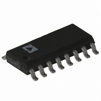
AD7524JRZ Analog Devices Inc, AD7524JRZ Datasheet - Page 2

AD7524JRZ
Manufacturer Part Number
AD7524JRZ
Description
IC DAC 8BIT MULTIPLYING 16-SOIC
Manufacturer
Analog Devices Inc
Datasheet
1.AD7524JNZ.pdf
(8 pages)
Specifications of AD7524JRZ
Data Interface
Parallel
Settling Time
250ns
Number Of Bits
8
Number Of Converters
1
Voltage Supply Source
Single Supply
Power Dissipation (max)
30mW
Operating Temperature
-40°C ~ 85°C
Mounting Type
Surface Mount
Package / Case
16-SOIC (3.9mm Width)
Resolution (bits)
8bit
Sampling Rate
4MSPS
Input Channel Type
Parallel
Supply Current
2mA
Digital Ic Case Style
SOIC
No. Of Pins
16
Lead Free Status / RoHS Status
Lead free / RoHS Compliant
Available stocks
Company
Part Number
Manufacturer
Quantity
Price
Part Number:
AD7524JRZ
Manufacturer:
ADI/亚德诺
Quantity:
20 000
Part Number:
AD7524JRZ-REEL
Manufacturer:
ADI/亚德诺
Quantity:
20 000
Company:
Part Number:
AD7524JRZ-REEL7
Manufacturer:
MOT
Quantity:
225
Part Number:
AD7524JRZ-REEL7
Manufacturer:
ADI/亚德诺
Quantity:
20 000
AD7524–SPECIFICATIONS
Parameter
STATIC PERFORMANCE
DYNAMIC PERFORMANCE
REFERENCE INPUT
ANALOG OUTPUTS
DIGITAL INPUTS
POWER SUPPLY
NOTES
1
2
3
4
5
Specifications subje
SWITCHING CHARACTERISTICS
Temperature ranges as follows: J, K, L versions: –40 C to +85 C
Gain error is measured using internal feedback resistor. Full-Scale Range (FSR) = V
Guaranteed not tested.
DAC thin-film resistor temperature coefficient is approximately –300 ppm/ C.
AC parameter, sample tested @ +25 C to ensure conformance to specification.
Resolution
Relative Accuracy
Monotonicity
Gain Error
Average Gain TC
DC Supply Rejection,
Output Leakage Current
Output Current Settling Time
(to 1/2 LSB)
AC Feedthrough
R
Output Capacitance
Input HIGH Voltage Requirement
Input LOW Voltage Requirement
Input Current
Input Capacitance
Chip Select to Write Setup Time
Chip Select to Write Hold Time
Write Pulse Width
Data Setup Time
Data Hold Time
I
DD
IN
J, A, S Versions
K, B, T Versions
L, C, U Versions
I
I
at OUT1
at OUT2
C
C
C
C
V
V
I
DB0–DB7
WR, CS
t
AD7524J, K, L, A, B, C
AD7524S, T, U
t
All Grades
t
AD7524J, K, L, A, B, C
AD7524S, T, U
t
AD7524J, K, L, A, B, C
AD7524S, T, U
t
All Grades
OUT1
OUT2
IN
CS
CH
WR
DS
DH
(Pin 15 to GND)
IH
IL
OUT1
OUT2
OUT1
OUT2
(Pin 1)
(Pin 2)
(Pin 1)
(Pin 1)
(Pin 2)
(Pin 2)
2
ct to change without notice
3
3
3
3
4
3
Gain/ V
A, B, C versions: –40 C to +85 C
S, T, U versions: –55 C to +125 C
3
5
DD
.
V
8
Guaranteed Guaranteed
0.08
0.002
400
0.25
0.25
5
20
120
30
30
120
+2.4
+0.8
5
20
170
0
170
135
10
1
100
170
170
135
1/2
1/2
1/2
2 1/2
40
50
50
1
DD
= +5 V V
Limit, T
8
0.02
0.001
250
0.25
0.25
5
20
120
30
30
120
+13.5
+1.5
5
20
100
100
0
100
100
60
60
10
2
100
A
1/2
1/4
1/8
1 1/4
10
50
50
1
DD
= +25 C
= +15 V V
(V
REF
8
Guaranteed
0.16
0.01
500
0.5
0.5
5
20
120
30
30
120
+2.4
+0.5
5
20
220
240
0
220
240
170
170
10
2
500
= +10 V, V
400
400
10
DD
1/2
1/2
1/2
3 1/2
40
Limit, T
= 5 V
REF
–2–
.
OUT1
MIN
V
8
Guaranteed
0.04
0.005
350
0.5
0.5
5
20
120
30
30
120
+13.5
+1.5
5
20
130
150
0
130
150
80
100
10
2
500
1/2
1/4
1/8
1 1/2
10
200
200
10
DD
, T
= V
= +15 V Units
MAX
OUT2
1
= 0 V, unless otherwise noted)
LSB max
LSB max
% FSR/% typ
pF max
pF max
pF max
V min
pF max
Bits
LSB max
LSB max
ppm/ C
% FSR/% max
nA max
nA max
ns max
% FSR max
% FSR max
k min
k max
pF max
V max
pF max
ns min
ns min
ns min
ns min
ns min
ns min
ns min
ns min
mA max
A max
A max
Test Conditions/Comments
Gain TC Measured from +25 C to
T
DB0–DB7 = 0 V; WR, CS = 0 V; V
DB0–DB7 = V
OUT1 Load = 100 , C
0 V; DB0–DB7 = 0 V to V
V
0 V; WR, CS = 0 V
DB0–DB7 = V
DB0–DB7 = 0 V; WR, CS = 0 V
V
V
V
See Timing Diagram
t
t
All Digital Inputs V
All Digital Inputs 0 V or V
WR
CS
V
REF
IN
IN
IN
MIN
DD
= 0 V or V
= 0 V
= 0 V
= t
= 10 V, 100 kHz Sine Wave; DB0–DB7 =
t
or from +25 C to T
WR
= 10%
CS
, t
CH
DD
DD
DD
0
; WR, CS = 0 V; V
; WR, CS = 0 V
IL
or V
EXT
IH
DD
DD
MAX
= 13 pF; WR, CS =
to 0 V.
REF
REF
= 10 V
= 10 V
REV. B


